Comparator Timing & Mixed-Signal Design
Why Comparator Propagation Delay Is Not Constant
A comparator datasheet may present propagation delay as a single number, but your circuit rarely operates under one fixed condition. Input overdrive, slew rate, common-mode voltage, supply level, temperature, output loading, and comparator architecture can all change how quickly a valid decision appears.
In this guide, you will see why comparator delay should be treated as an operating-dependent distribution rather than a fixed specification—and how to build timing guardbands that remain reliable across real system conditions.
Input Overdrive
Decision-Time Tails
PVT Conditions
Timing Guardbands
tPD
Core Engineering Principle
Comparator propagation delay is not simply a device constant. It results from the input condition, internal decision mechanism, output interface, and the point at which your next stage considers the result valid.
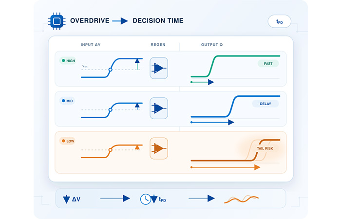
Smaller input overdrive can produce a slower and less predictable decision.
A Fast Comparator Is Not Always Fast
Suppose you select a comparator with a typical propagation delay of 4 ns. During bench testing, most transitions arrive close to that value—but a small number of decisions take significantly longer, especially when the input difference is small or the signal crosses the threshold slowly.
4 ns
Typical Does Not Mean Universal
The published number describes performance under a defined test condition. It does not automatically guarantee the same delay for every input amplitude, signal slope, temperature, supply condition, or output interface in your design.
To understand whether a comparator is genuinely fast enough for your system, you need to look beyond the headline specification and examine the conditions behind the measurement.
ΔV
Fixed Test Overdrive
Datasheet tPD is usually measured with a specified input overdrive. Your minimum system overdrive may be much smaller.
PVT
Defined Operating Point
The published delay may apply only at a particular VDD, temperature, common-mode voltage, and output load.
∿
Variable Input Behavior
Real signals do not always arrive with the same amplitude or slope. A slow threshold crossing can widen timing uncertainty.
p99
Tail Decisions Matter
A normal average delay does not prove that the slowest decisions will fit inside your capture window.
The Question Your Timing Budget Must Answer
Not simply “How fast is this comparator?” but “How fast and predictable is it under the smallest overdrive and worst operating conditions your system will encounter?”
What Comparator Propagation Delay Actually Measures
Before you compare devices or build a timing budget, you need to define exactly where the delay measurement begins and where it ends. Without those reference points, two propagation-delay values may describe very different conditions.
Propagation Delay
tPD
=
toutput valid
−
tinput reference
IN
Input Reference Point
You need to know what input event starts the timer:
-
Crossing the nominal switching threshold
-
Reaching the zero-differential point
-
Reaching a specified datasheet test voltage
OUT
Output-Valid Point
You also need to define when the result becomes usable:
-
Reaching 50% of the output swing
-
Crossing the next stage’s VIH or VIL limit
-
Reaching sufficient differential swing for a latch or flip-flop
The distinction matters because the comparator may have completed its internal decision before the output reaches a level that your downstream logic can safely capture. For your system, the relevant value is therefore the delay to the actual digital-valid point, not necessarily the first visible output movement.
Before using a published tPD value, also confirm:
tPLH or tPHL
Average or individual delay
Capacitive output load
Termination network
Pull-up resistance
|
Test Field
|
What You Need to Confirm
|
Why It Matters
|
|
Input overdrive
|
Input amplitude beyond the effective threshold
|
Directly affects how quickly the internal decision develops
|
|
Input slew rate
|
Speed at which the input crosses the threshold
|
Slow slopes increase timing uncertainty near the threshold
|
|
Common-mode voltage
|
Input common-mode operating point
|
Influences input-stage gm, headroom, offset, and speed
|
|
Supply voltage
|
Nominal VDD or guaranteed minimum VDD
|
Lower VDD can reduce internal gain and output drive
|
|
Temperature
|
Room temperature or required temperature corner
|
Transconductance, offset, and propagation delay can all drift
|
|
Output load
|
Capacitance, termination, pull-up, and logic interface
|
Determines when the output reaches a usable logic level
|
|
Valid threshold
|
50% output swing or actual VIH/VIL requirement
|
Defines when your downstream stage can safely capture the result
|
✓
Practical rule: Compare propagation-delay numbers only after confirming that the input overdrive, VDD, common mode, temperature, output load, and output-valid threshold are relevant to your circuit.
Input Overdrive: The First Variable Behind tPD
When you evaluate comparator timing, input overdrive is usually the first condition to check. It describes how strongly the input asks the comparator to choose one state over the other at the decision moment.
A larger overdrive gives the internal circuitry a clearer initial imbalance. A smaller overdrive places the decision closer to the comparator’s offset and noise floor, where the result usually takes longer to develop and becomes less predictable.
Differential Comparator
VOD
=
|VINP
−
VINN|
For a differential comparator, overdrive is the effective voltage difference between the positive and negative inputs when the decision is being made.
Single-Ended Threshold Detection
VOD
=
|VIN
−
VTH|
For single-ended threshold detection, overdrive is the amount by which the input has moved beyond the effective switching threshold.
Clear Decision
Large Overdrive
-
✓
The internal differential signal develops quickly.
-
✓
The output usually reaches its valid state sooner.
-
✓
Noise and offset are small relative to the input difference.
-
✓
The delay distribution is normally narrower.
Condition Sensitive
Medium Overdrive
-
•
Delay becomes more sensitive to supply and temperature.
-
•
Input slope and output load have a more visible effect.
-
•
Typical tPD may still be useful as a reference.
-
•
You still need to verify relevant PVT corners.
Tail-Risk Region
Small Overdrive
-
!
The initial internal differential is very small.
-
!
Noise, offset, and device mismatch become more influential.
-
!
The decision generally requires more time.
-
!
The delay distribution may develop a pronounced right-side tail.
Δ
Do Not Confuse Signal Amplitude with Decision Overdrive
Your signal can have a large total amplitude while still presenting only a tiny differential at the critical decision instant. What matters is the effective input difference inside the comparator’s sensitive region.
Why Delay Becomes a Distribution Near the Threshold
When overdrive is comfortably larger than the comparator’s uncertainty sources, most decisions follow a relatively narrow timing range. As the input approaches the threshold, those same uncertainty sources become comparable with the useful differential signal.
This means that even when you repeat what appears to be the same input condition, the output may not become valid at exactly the same time. Instead of one fixed delay, you observe an operating-dependent delay distribution.
What Gains Influence at Small Overdrive
σ
Input-Referred Noise
Δ
Device Mismatch
VOS
Offset Voltage
∿
Supply Ripple
CLK
Clock or Reset Injection
dV/dt
Input Slope Variation
T°
Temperature-Dependent Gain
Conceptual Delay Profiles
Wider profiles indicate greater decision-time uncertainty.
Delay →
p50
Half of the observed decisions complete before this time, and half complete after it.
p99
Ninety-nine percent of the measured decisions complete before this point.
p999
The 99.9th-percentile point is useful for higher-reliability analysis but requires a much larger sample set.
Tail Flag
Records whether a small group of decisions extends significantly beyond the main delay distribution.
Interpreting the Long Tail Correctly
Near a balanced input condition, some comparator architectures can produce a metastability-like decision-time tail. This describes the unusually long decision behavior without assuming that every comparator enters the same classical metastable state as a flip-flop. The exact mechanism depends on the architecture and operating condition.
✓
For your timing budget, the average delay is not enough. You need to know where the p99 or required tail percentile falls under the smallest expected overdrive—and place the capture instant beyond it with an explicit guardband.
Comparator Architecture Changes the Delay Mechanism
Two devices can publish similar propagation-delay values and still behave very differently in your circuit. The reason is that comparator architectures do not establish, amplify, and deliver a decision in the same way.
Propagation delay must therefore be interpreted in the context of circuit architecture. The broader design0 26px 0;font-size:17px;line-height:1.9;color:#486581;”>
Propagation delay must therefore be interpreted in space of
Comparators & Schmitt Triggers
includes continuous-time comparators, hysteretic threshold detectors, and clocked regenerative circuits. Each architecture responds differently to input overdrive, noise, slow input slopes, and timing constraints.
∿
Asynchronous Decision
Continuous-Time Comparator
This architecture continuously monitors the input and responds without waiting for a separate evaluate clock.
-
•
Responds asynchronously to input changes.
-
•
Typically uses continuous bias current.
-
•
Delay depends on input-stage gain, compensation, output drive, and overdrive.
-
•
Fits threshold detection, zero crossing, and protection circuits.
VH
Hysteretic Decision
Schmitt Trigger
A Schmitt trigger uses two switching thresholds to prevent a noisy or slowly moving input from repeatedly changing the output state.
-
•
Uses separate rising and falling thresholds.
-
•
Handles slow, noisy, or chatter-prone inputs.
-
•
Improves noise immunity through hysteresis.
-
•
Is not ideal when you require one precise conversion threshold.
CLK
Sampled Decision
Clocked Regenerative Comparator
This architecture waits for a defined evaluate phase and then uses positive feedback to amplify a small differential input.
-
•
The clock defines the decision window.
-
•
Energy is consumed mainly during evaluation.
-
•
Positive feedback provides fast regeneration.
-
•
Requires control of reset memory, kickback, and small-overdrive tails.
|
Architecture
|
Decision Mode
|
Main Advantage
|
Delay Concern
|
Natural Application
|
|
Continuous-time comparator
|
Asynchronous
|
Immediate monitoring
|
Static power and overdrive sensitivity
|
Threshold and zero-crossing detection
|
|
Schmitt trigger
|
Asynchronous with hysteresis
|
Noise immunity
|
Different rising and falling thresholds
|
Slow or noisy digital interfaces
|
|
Regenerative latch
|
Clocked
|
Regenerative latch
High speed and low energy per decision
|
Reset quality and small-OD tails
|
SAR ADC, TDC, and sampled decisions
|
✓
For your design, compare more than the headline tPD. First identify whether you need continuous monitoring, hysteretic noise rejection, or a clocked low-energy decision—and then evaluate delay under the conditions that matter to that architecture.
Why Regenerative Latches Develop Long Decision-Time Tails
This behavior becomes especially important in clocked mixed-signal systems. A
Regenerative (StrongARM-Type) Dynamic Latch Comparator
resets its internal nodes before evaluation and then uses positive feedback to amplify a small differential input into a full-swing digital decision.
The architecture can be both fast and energy-efficient, but its decision time becomes increasingly sensitive as input overdrive approaches zero. To understand that behavior, you need to separate the decision into its reset, evaluate, regeneration, and capture stages.
RST
Reset and Precharge Define the Starting Point
Before each comparison, the internal nodes must return to a known and repeatable condition. If they do not, the next decision may begin with an unintended imbalance.
Internal nodes must return to a repeatable initial state.
Incomplete reset can leave residual charge behind.
The previous decision can then influence the next result.
Reset width and clock duty cycle change the effective starting condition.
Evaluate and Regenerate
Once evaluation begins, positive feedback causes the internal differential voltage to grow approximately exponentially. The simplified relationships below capture the timing behavior that matters to your system.
Differential Growth
ΔV(t) ≈ ΔV0 · et/τ
Time to a Valid Decision
tdecision
≈ τ ln
Vtarget
ΔV0
ΔV0 is the effective initial differential when regeneration begins.
A smaller ΔV0 requires more time to reach the same valid output level.
Higher gm and lower internal capacitance can shorten the effective time constant τ.
Noise, mismatch, and residual reset charge can also change the effective ΔV0.
Capture Timing Must Follow the Valid Decision
Your timing budget must distinguish every stage between the evaluate edge and the final digital capture. Treating them as one ideal event can hide a real setup-time failure.
Evaluate Start
Output Crossing
Digital Valid
FF Setup Time
Final Capture
Early Fixed Capture
If the sampling point falls inside the small-overdrive delay tail, a low-probability but real late decision can be captured incorrectly.
Tail-Aware Capture
Place the capture point beyond the verified delay percentile, then add margin for setup time, clock jitter, path skew, and operating-condition variation.
tPD
The correct capture time is not based on the typical regeneration delay. It must cover the required tail percentile at the smallest expected ΔV0, under the worst relevant reset, supply, temperature, loading, and clock conditions.
Other Conditions That Move Propagation Delay
Input overdrive is a primary timing variable, but it is not the only one. The same comparator can produce a different delay when you change the signal slope, common-mode operating point, supply voltage, temperature, output load, or source impedance.
To predict whether the result will arrive inside your capture window, you need to evaluate the complete input-to-valid-output path under the conditions your finished system will actually experience.
dV/dt
Signal Transition
Input Slew Rate
A slowly moving input remains inside the comparator’s sensitive threshold region for longer. During that interval, offset, noise, and supply disturbance have more opportunity to change the apparent switching time.
Slow inputs spend more time close to the threshold.
Voltage uncertainty can become timing jitter.
Noise may create repeated threshold crossings or output chatter.
A Schmitt trigger can stabilize some noisy inputs, but its hysteresis changes the switching threshold.
VICM
Input Common-Mode Voltage
Your input common-mode operating point changes the voltage headroom available to the input transistors and can alter their effective transconductance.
-
•
Common-mode voltage changes input-stage gm and headroom.
-
•
Speed and offset may degrade as the input approaches either supply rail.
-
•
A rail-to-rail input claim does not guarantee identical delay at every common-mode point.
PVT
Supply Voltage and Temperature
Supply and temperature change the internal gain, device current, regeneration strength, and output-drive capability that determine how quickly a valid result develops.
-
•
Lower VDD can weaken internal gain and output drive.
-
•
Higher temperature commonly reduces carrier mobility and gm.
-
•
Cold conditions may also change startup, offset, and output behavior in some architectures.
CLOAD
Output Loading
The internal comparison may be complete before the external output reaches a level that your next logic stage can safely recognize.
-
•
Higher output capacitance increases valid-level delay.
-
•
Open-drain outputs also depend on pull-up resistance and bus capacitance.
-
•
The system may still be waiting even after the internal decision has finished.
RSRC
Source Impedance
The impedance driving the comparator interacts with its input capacitance and any switching disturbance returned from the input stage.
-
•
High source impedance can create additional RC settling delay.
-
•
Clocked comparators may disturb high-impedance inputs through kickback.
-
•
A low-impedance laboratory source may not represent your sensor or CDAC interface.
|
Variable
|
Typical Effect
|
Failure Signature
|
| Lower overdrive |
Longer and wider delay distribution |
Late or intermittent decisions |
| Slower input slope |
More timing uncertainty |
Jitter or output chatter |
| Near-rail common mode |
Reduced input-stage headroom |
Slow or biased decisions |
| Lower VDD |
Weaker gain and output drive |
Expanded delay tail |
| Higher output load |
Longer valid-level time |
Downstream logic captures too early |
| Higher source impedance |
More settling and kickback sensitivity |
Input-dependent delay or spurs |
✓
Your useful specification is not tPD under one ideal condition. It is the delay to a valid output across the input, PVT, source, and loading envelope your system must support.
How Timing Errors Appear in Real Systems
Comparator delay rarely appears in a finished product as a simple “late output.” It is translated by the surrounding architecture into conversion errors, timing jitter, unstable encoding, false triggers, or intermittent failures.
Conversion Timing
SAR ADC
SMALL FINAL-BIT OVERDRIVE
In a SAR ADC, the CDAC node must complete its switching and settling before the comparator enters the valid evaluate window. Later conversion steps often present smaller input differences, making the final decisions more sensitive to delay tails.
CDAC Switching
→
Input Settling
→
Evaluate
→
SAR Capture
A late output can cause the SAR logic to capture the wrong decision.
Kickback can disturb the CDAC top-plate voltage.
Switching, settling, evaluate, and capture phases require controlled non-overlap.
Missing Codes
DNL / INL Degradation
Code-Dependent Spurs
ENOB / SFDR Loss
Intermittent Errors
Arrival-Time Decision
TDC and Arbiter
- •Near-simultaneous edges create a very small effective initial difference.
- •Delay tails become time uncertainty.
- •A/B path mismatch creates systematic time offset.
- •The result requires a defined synchronization strategy.
Timestamp Decision
ToF and Time Pick-Off
- •Slow edges convert voltage noise into timing jitter.
- •Threshold uncertainty widens the timestamp distribution.
- •Supply bounce and clock feedthrough can create correlated timing bias.
Headroom-Limited Decision
Low-VDD Threshold Detection
- •The comparator may switch but still miss the required valid-output time.
- •Near-rail thresholds increase delay and offset risk.
- •Verify VDDmin, Tmax, and VICM corners.
| System |
Critical Condition |
Timing Consequence |
Main Verification |
| SAR ADC |
Small final-bit overdrive |
Wrong code capture |
tPD tail and kickback |
| TDC / arbiter |
Near-simultaneous arrivals |
Time offset or unstable encoding |
Delay histogram and path matching |
| ToF pick-off |
Slow noisy edge |
Timestamp jitter |
Slope and threshold uncertainty |
| Low-VDD detector |
Weak headroom |
Late or incomplete transition |
VICM × VDD timing map |
The same comparator delay can become a wrong ADC code, a TDC time offset, a ToF timestamp spread, or a missed low-voltage event. Your verification metric must therefore match the system-level failure mode.
Why Typical tPD Is Not Enough for Component Selection
A typical propagation-delay value is useful for initial screening, but it does not tell you whether a comparator will meet timing at your minimum overdrive, lowest supply, temperature extremes, common-mode corners, and actual output load.
Before you approve a device, look for timing information that lets you reconstruct the comparator’s real operating envelope.
Data to Check Before Selecting a Comparator
tPD versus input overdrive
Rising and falling delay
VDDmin timing
Hot and cold timing
VICM corner behavior
Input slew-rate assumptions
Output load and termination
Maximum-delay conditions
Latch-enable or clock timing
Delay dispersion or histogram data
Questions to Ask the Vendor
If the datasheet does not provide enough detail, ask for the conditions behind the number rather than requesting another typical value.
?
What input overdrive was used to specify propagation delay?
?
Is a tPD-versus-overdrive curve available?
?
Is the maximum delay guaranteed across temperature and supply voltage?
?
What output threshold defines the published propagation delay?
?
Does the device exhibit long-tail behavior near zero overdrive?
?
What input source impedance was assumed during characterization?
?
Are latch-enable setup, hold, recovery, and output-valid times specified?
Normalize
Match overdrive, PVT, load, and valid-level conditions.
→
Characterize
Review distributions and tail behavior, not only averages.
→
Guardband
Set capture timing beyond the required worst-case percentile.
MAX
Even when a datasheet provides a maximum tPD, confirm which overdrive, common-mode, temperature, supply, slew-rate, and output-load conditions that maximum actually covers. A guaranteed maximum outside your operating conditions is not yet a timing guarantee for your system.
Building a Tail-Aware Timing Budget
A reliable timing budget must cover more than the comparator’s typical propagation delay. Your available decision window must also include input settling, the required delay percentile, output-valid time, downstream setup time, clock-path uncertainty, and an explicit engineering margin.
The objective is to place the final capture point beyond the verified decision-time tail, not merely beyond the average response.
Complete System Budget
Tavailable
≥
Tsettling
+
tdecision,p99
+
Toutput-valid
+
Tsetup
+
Tskew
+
Tmargin
Clocked Comparator Budget
Tcapture
−
Tevaluate
≥
tPD,p99
(ODmin, PVTworst)
+
Tsetup
+
Tguardband
i
Define tPD consistently. If your measured tPD already ends at the actual digital-valid threshold, do not add the same output-valid transition time a second time.
Tail-Aware Capture Path
Input Settling
→
Evaluate
→
Decision p50
→
Decision p99
→
Output Valid
→
Setup
→
Capture
Verified Tail Coverage + Clock Jitter + Path Skew + Explicit Guardband
Build the Budget from Your Worst Real Condition
1
Define the minimum expected input overdrive
Use the smallest differential your system can present during a valid decision—not the nominal or maximum signal amplitude.
2
Define the worst operating envelope
Include minimum VDD, temperature extremes, common-mode corners, source impedance, and the actual output load.
3
Define what “output valid” means
Use the actual VIH, VIL, or differential-input requirement of the downstream latch or logic stage.
4
Measure or simulate a delay distribution
Record repeated decisions and inspect the tail instead of relying only on the average propagation delay.
5
Choose the percentile that matches product risk
A development prototype, consumer product, industrial controller, and safety-related system may require different tail coverage.
6
Add clock and interface uncertainty
Include clock jitter, path skew, setup time, and any uncertainty in the evaluate start condition.
7
Preserve an explicit guardband
Do not consume every theoretical nanosecond of margin during nominal design or early optimization.
GB
There is no universal 20% or 30% comparator guardband. Your timing guardband should come from the measured or simulated worst-condition delay distribution, the required failure probability, and the reliability target of your system.
Simulation and Bench Verification
A useful verification plan should let you compare simulation, layout-aware analysis, bench results, and production guardbands using the same conditions and logging fields. That consistency makes it much easier to identify whether a failure comes from overdrive, PVT, loading, clock behavior, or reset memory.
Simulation Plan
Overdrive Sweep
Small OD
Tail-risk condition
Medium OD
Condition-sensitive region
Large OD
Predictable reference
Repeat each overdrive bin across the operating conditions that matter to your design:
VDD nominal / minimum
Cold / room / hot
Mid-range / near-rail VICM
Light / expected / worst load
Monte Carlo and Mismatch
Mean delay
Standard deviation
p99 estimate
Offset distribution
Tail flag
Decision failure
Use enough samples for the percentile you intend to claim. Rare-tail estimates require substantially more trials than mean or standard-deviation estimates.
Clocked Comparator Checks
Reset width
Duty cycle
Clock edge rate
Clock swing
Evaluate-to-capture time
Look for timing or decision bias that moves with reset duration, clock swing, edge rate, or the previous output state.
Bench Plan
Primary Timing Test
Delay Versus Overdrive
- •Hold common mode and output load constant.
- •Sweep the input overdrive.
- •Capture enough repeated events at each point.
- •Report p50, p99, and the observed tail.
Signal-Shape Test
Input Slew Rate
- •Hold input amplitude constant.
- •Change the threshold-crossing speed.
- •Inspect delay, jitter, and repeated transitions.
Operating-Corner Test
PVT and Loading
- •Change supply voltage and temperature.
- •Apply the actual expected output load.
- •Recalculate delay using the real VIH or VIL threshold.
Dynamic Comparator Test
Clock and Reset Sensitivity
- •Sweep reset width and duty cycle.
- •Change clock edge rate and swing.
- •Check whether the previous decision influences the next result.
Recommended Logging Fields
architecture:
part_number:
vdd:
temperature:
vicm:
input_overdrive:
input_slew_rate:
output_load:
tpd_rising_p50:
tpd_rising_p99:
tpd_falling_p50:
tpd_falling_p99:
tail_flag:
clock_condition:
reset_width:
capture_point:
guardband:
✓
Use the same field names across simulation and bench testing. When a discrepancy appears, you can then map it directly to overdrive, PVT, loading, reset, clock, or tail behavior.
Match the Mitigation to the Dominant Delay Mechanism
Once you identify a timing problem, the next step is not automatically to select the fastest available comparator. You first need to determine whether the dominant mechanism is small overdrive, weak regeneration, slow input slope, loading, headroom, reset memory, kickback, or clock uncertainty.
Observe
Identify the actual failure signature.
→
Localize
Find the dominant electrical mechanism.
→
Mitigate
Apply the lightest fix that meets the target.
|
Dominant Problem
|
Appropriate Response
|
Main Trade-Off
|
| Small-overdrive tail |
Add decision time or preamplification |
More latency, power, or area |
| Weak regeneration |
Increase gm or reduce internal loading |
Power and design complexity |
| Slow noisy input |
Signal conditioning or hysteresis |
Threshold accuracy |
| Heavy output load |
Add a buffer or reduce capacitance |
Extra stage delay and power |
| Near-rail input |
Select a suitable input architecture |
Device choice or supply change |
| Reset memory |
Increase and balance reset action |
Shorter evaluate window |
| Kickback |
RC damping, isolation, or a preamplifier |
Settling, noise, power, and area |
| Clock uncertainty |
Improve routing and capture guardband |
More timing budget |
!
Avoid Treating Every Symptom the Same Way
Do not automatically choose the fastest comparator for a slow, noisy input, and do not add hysteresis simply because the output chatters. The correct response must match the dominant delay or uncertainty mechanism.
In a precision ADC, hysteresis may reduce chatter while converting a random timing problem into a deterministic threshold error. Always verify the impact on offset, linearity, settling, and the required conversion threshold.
Selection & Design Review
Engineering Checklist Before Selecting a Comparator
Use this checklist to define the conditions your comparator must handle before you compare headline speed specifications. Your goal is to select a device that remains fast, predictable, and digitally valid throughout your actual operating envelope.
-
What is the minimum input overdrive your system will produce?
-
What is the slowest input slew rate at the switching threshold?
-
Which input common-mode range must the comparator support?
-
Is your source low impedance, or is it sensitive to sampling disturbances?
-
Can your input network tolerate comparator kickback?
-
Is your decision asynchronous or clocked?
-
Which event defines the start of the decision interval?
-
When must the output become digitally valid for the next stage?
-
What setup time does the downstream logic require?
-
Which delay percentile—such as p99 or p99.9—must your timing budget cover?
-
What are your required VDDmin and VDDmax limits?
-
Which cold and hot temperature corners must be supported?
-
What output load and logic interface will the comparator drive?
-
Does your application require near-rail input operation?
-
Must the device recover within a defined time after shutdown or reset?
✓
Verification Conditions
-
Is tPD-versus-overdrive data available?
-
Have you tested the smallest expected overdrive?
-
Have you recorded both p50 and p99 delay?
-
Have you checked whether reset or decision history changes the result?
-
Is your final timing guardband based on measured or validated data?
i
If one of these questions remains unanswered, treat the corresponding timing margin as unverified. A typical datasheet value cannot close a system-level timing budget when your minimum overdrive, valid-output threshold, or worst PVT condition is still unknown.
Final Takeaway
Design for the Decision You Must Capture—not the Typical Number in the Datasheet
A comparator’s published propagation delay is a useful starting point, but it is not a complete timing guarantee. As your input overdrive decreases, the decision usually becomes slower and less predictable. Input slew rate, common-mode voltage, supply, temperature, loading, and comparator architecture can reshape the result even further.
1
Characterize the real envelope
Verify delay across your actual overdrive, slew rate, VICM, VDD, temperature, and loading conditions.
2
Measure the delay distribution
Treat small-overdrive timing as a distribution that may include rare, long decision-time events.
3
Protect the capture point
Place capture beyond the verified decision-time tail and preserve an explicit, evidence-based guardband.
The fastest comparator under typical datasheet conditions is not necessarily the comparator that gives you the most reliable decision in the finished system.
Comparator Timing FAQ
Frequently Asked Questions
Use these answers to clarify how input conditions, comparator architecture, and system timing affect the delay you must account for in your design.
What is propagation delay in a comparator?
Comparator propagation delay is the time between a defined input event and the moment the output reaches a valid level. The result depends on how you define the input reference point and output-valid threshold, as well as the applied overdrive, slew rate, supply voltage, temperature, and output loading.
What is comparator input overdrive?
Input overdrive is the amount by which your input exceeds the effective switching threshold. In a differential comparator, it is commonly represented by the voltage difference between the positive and negative inputs at the decision moment.
Why does propagation delay decrease as overdrive increases?
A larger overdrive creates a stronger initial imbalance inside the comparator. Its internal gain stages or regenerative nodes therefore require less time to develop enough voltage difference to switch the output into a valid state.
Why is comparator propagation delay not constant?
Propagation delay changes because the comparator’s internal gain, charging current, regeneration strength, and output transition depend on your input and operating conditions. Overdrive, input slope, common mode, VDD, temperature, architecture, and output load can all move the result.
What happens when comparator overdrive approaches zero?
The initial differential signal becomes comparable with offset, device noise, and mismatch. Your decisions usually take longer, the delay distribution becomes wider, and regenerative architectures may develop a metastability-like decision-time tail.
Does input slew rate affect comparator propagation delay?
Yes. A slow input slew rate keeps your signal near the switching threshold for longer, allowing noise and threshold uncertainty to create greater timing variation. Slow slopes can also cause output chatter unless you use suitable hysteresis or signal conditioning.
How should comparator propagation delay be measured?
You should measure propagation delay across several overdrive levels while controlling common mode, slew rate, supply voltage, temperature, and output load. Use repeated captures to calculate p50 and p99 delay instead of relying on a single transition.
How much timing guardband should a comparator have?
There is no universal percentage. Your timing guardband should be based on the worst required overdrive, PVT condition, output load, delay percentile, clock jitter, path skew, and downstream setup time.
When should a Schmitt trigger be used instead of a comparator?
A Schmitt trigger is useful when your slow or noisy signal causes repeated transitions and precise single-threshold accuracy is not required. Its hysteresis improves noise immunity, but it also creates different rising and falling thresholds.
Why are StrongARM comparators commonly used in SAR ADCs?
StrongARM comparators combine fast positive-feedback regeneration with low energy per decision because they operate dynamically during a clocked evaluation phase. When you integrate one into a SAR ADC, the main risks to verify include small-overdrive delay tails, offset, reset memory, and input kickback.
Practical reminder: Your timing budget should be based on the conditions your finished system will actually encounter—not only the typical propagation-delay value shown at one datasheet test point.