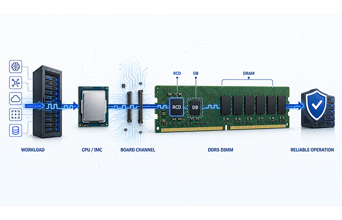
How DDR5 Signal Integrity Shapes Server Reliability
Data Center Memory Reliability
How DDR5 Signal Integrity Shapes Server Reliability
DDR5 gives AI, HPC, cloud, virtualization, and in-memory database platforms the bandwidth and capacity they need. But as data rates, capacity, and module population increase, server memory becomes more sensitive to jitter, skew, reflections, crosstalk, loading, and temperature-driven drift.
AI & HPCCloud InfrastructureTiming MarginThermal Stability
Conceptual signal path: Data center workload → CPU/IMC → board channel → DDR5 RDIMM → RCD/DB → DRAM → reliable operation.
The Short Answer
DDR5 signal integrity shapes server reliability because every clock, command, address, and data signal must still arrive within a valid timing and voltage window after passing through the processor interface, board channel, DIMM connector, module-level devices, and DRAM loads. As data rates, capacity, and module population increase, maintaining that window becomes progressively more difficult.
01
Peak bandwidth is not enough
Data centers need bandwidth that remains stable and repeatable through sustained workloads, changing temperatures, and higher DIMM populations.
02
A short pass is not proof of margin
A system that trains during a cold boot or passes a brief test may still fail after heat builds or the weakest slot is stressed.
03
ECC is protection, not restored margin
ECC can detect or correct supported errors, but it cannot recreate timing or voltage margin that has already been lost.
What insufficient DDR5 margin may look like
Memory training failureCorrectable ECC eventsUncorrectable errorsParity or ALERT eventsSlot-specific instabilityHot-only failureApplication crash or downtime
Why Server Memory Reliability Matters at Data Center Scale
At data center scale, reliable memory means more than reaching a high transfer rate during initial qualification. The bandwidth available during a short test must remain usable when the server is fully populated, thermally settled, and running demanding workloads for hours or days.
Your actual memory requirements depend on the workload. Some environments prioritize sustained bandwidth, while others depend more heavily on capacity, latency, data integrity, or consistency across thousands of deployed servers.
AIAI/ML Training
Requires high bandwidth under sustained utilization. Continuous data movement and thermal load can expose a channel that appeared stable during a short test.
HPCHigh-Performance Computing
Depends on predictable bandwidth and low latency across long calculations. Intermittent memory errors can invalidate results or force expensive job restarts.
DBIn-Memory Databases
Combine large capacity with strict data-integrity and latency requirements. Even infrequent instability can affect transactions, availability, and recovery time.
CLDCloud Hosting
Places high DIMM density, multi-tenant activity, and fleet-wide consistency in the same system. A marginal configuration can become a large operational problem at scale.
VMVirtualization
Requires substantial capacity while many different workloads operate simultaneously. Stable channel balance matters as utilization changes throughout the day.
RTReal-Time Analytics
Relies on consistent latency and stable throughput. Brief pauses, retries, or corrected-error bursts can still affect time-sensitive processing.
What changes as your server platform scales?
More CPU coresIncrease pressure on memory bandwidth per core.
Higher capacityMay require more ranks, denser devices, or a larger DIMM population.
Maximum speedMay not remain available in the platform’s highest-capacity configuration.
This is why server memory reliability affects more than benchmark performance. It influences service availability, maintenance time, qualification effort, replacement planning, and the total cost of keeping infrastructure operational.
What Signal Integrity Means in a DDR5 Server
DDR5 signal integrity means that clock, command, address, data, and strobe signals still reach their receivers inside a valid voltage and timing decision window after traveling through the processor interface, board routing, DIMM connector, module-level circuitry, and DRAM loads.
A signal does not need to look electrically perfect. It needs to remain distinguishable at the receiver and arrive while the receiver is able to sample it correctly. That usable region can be understood through two related dimensions: voltage margin and timing margin.
VVoltage Margin
The vertical electrical space that allows the receiver to distinguish one logic state from another.
•Signal amplitude
•Noise and power-related disturbance
•Overshoot and undershoot
•Crosstalk
•Reflections from discontinuities
TTiming Margin
The horizontal time window in which a signal remains stable enough to be sampled correctly.
•Setup and hold margin
•Jitter
•Skew
•Duty-cycle distortion
•Delay variation and thermal drift
How Margin Appears in an Eye DiagramConceptual illustration — not measured DDR5 data
In a conceptual eye diagram, increased noise closes the eye vertically, while jitter and skew reduce the horizontal opening. The sampling point must remain inside the usable region. However, an open eye under one condition does not prove that every slot, temperature, module population, or operating duration will preserve the same margin.
Why DDR5 Leaves Less Room for Signal Error
DDR5 increases server memory bandwidth and efficiency, but higher operating rates make each portion of the timing budget more valuable. The first mainstream DDR5 server platforms began at 4800 MT/s, and later generations continue to move higher.
As the data rate rises, the Unit Interval becomes shorter. The same absolute amount of jitter or delay variation therefore consumes a larger percentage of the available time window.
Shorter Timing Window
Higher transfer rates shorten each UI, making jitter, skew, and propagation-delay variation more visible.
Power Integrity
DDR5 uses 1.1V DRAM supplies and on-module power management. This improves local control but does not remove noise, droop, or thermal considerations.
Capacity and Population
More ranks, denser devices, and higher DIMM population increase loading, heat, and the number of conditions that must be qualified.
DDR5 also divides the DIMM into two independent 32-bit data subchannels. On server ECC RDIMMs, each subchannel commonly includes eight additional ECC bits, producing two 40-bit subchannels. This improves concurrency, but it also creates a more structured architecture that must remain consistent across channels, ranks, slots, and thermal conditions.
Engineering Dimension
DDR4 Environment
DDR5 Environment
Reliability Impact
Data rate
Lower platform rates
Higher and continuing to scale
Shorter UI makes jitter a larger part of the timing budget.
DRAM voltage
1.2V
1.1V
Power integrity and noise control require closer attention.
DIMM channels
Single 64-bit module structure
Two independent subchannels
Concurrency improves while architecture and validation become more structured.
Power regulation
Primarily on the motherboard
PMIC located on the DIMM
Local regulation improves, but module power and heat must still be managed.
On-die ECC
Not a standard DDR4 DRAM feature
Built into DDR5 DRAM
Protects the internal array but does not protect the external memory bus.
Validation focus
Skew and thermal drift remain important
Worst-slot and hot-soak behavior become more visible
Average results can hide the branch that actually limits reliability.
DDR5 is not inherently unreliable. It is simply less forgiving when routing, loading, power, temperature, or validation consistency consumes too much of the remaining margin. The real question is not whether a platform can reach a target rate once, but whether it can preserve repeatable operating margin across the conditions in which your servers will actually run.
The DDR5 Server Memory Signal Chain
When you evaluate DDR5 signal integrity, it helps to stop thinking of the DIMM as an isolated component. Every signal must travel through a complete electrical path before a DRAM device can interpret it correctly.
The path begins inside the processor, crosses the motherboard and connector, passes through module-level interface devices, and finally reaches the DRAM packages. Weak margin at any point can affect the behavior you observe at the system level.
CPU
Memory Controller / PHYHost-side signal source and receiver
→
PCB
Motherboard RoutingTraces, vias, topology and return paths
→
DIMM
DIMM ConnectorMechanical and electrical transition point
→
IC
Module-Level ICsControl, buffering, power and management
→
DRAM
DRAM DevicesFinal signal destinations on the module
This complete path carries several different classes of signals. They interact inside the same memory subsystem, but they do not all behave in the same way or rely on the same supporting devices.
System Domain
Signals or Functions
Related Devices
Common Weak-Margin Signs
CK/CA Control PathControl Signals
Clock, command and address
RCD
Training failure, parity events and slot sensitivity
DQ/DQS Data PathData Signals
Read/write data and data strobe
DRAM, DFE and DB
ECC events, data errors and eye closure
Power and ThermalOperating Conditions
VDD, VDDQ, local regulation and temperature
PMIC and temperature sensors
Hot-only failure, voltage variation and thermal drift
Sideband ManagementConfiguration and Telemetry
SPD data, configuration and monitoring
SPD Hub and I3C
Inconsistent readback, configuration or device visibility
How you should read this architecture
Different paths, different symptomsA CK/CA failure may look different from a DQ/DQS data-path failure.
PMIC supports power integrityIt regulates local power; it does not re-time the CK/CA control path.
ECC belongs to the RAS layerIt can detect or correct supported errors but does not restore lost signal margin.
Sensors provide visibilityTemperature data helps you respond to heat, but monitoring alone does not provide cooling.
DDR5 Features Protect Different Parts of the System
DDR5 introduces several architectural features that improve bandwidth, efficiency, power control, error handling, and module management. The important point for your design is that these features do not all solve the same problem.
A feature that strengthens the data path cannot automatically correct a control-path problem. Likewise, error correction can reduce the effect of some faults without removing the electrical condition that caused them.
DDR5 Feature
What It Actually Supports
What It Cannot Guarantee
Dual SubchannelsARCHITECTURE
Improves parallel access, scheduling efficiency and channel utilization.
Does not directly guarantee signal integrity or stable operating margin.
DFEDATA PATH
Helps the receiver compensate for post-cursor ISI on the data path.
Does not organize or re-time CK/CA fanout across the DIMM.
PMICPOWER
Provides local voltage regulation and improves control over module power delivery.
Does not eliminate every source of noise, voltage variation or heat.
On-Die ECCRAS
Corrects supported errors within the internal DRAM array.
Does not protect the external path between the DIMM and CPU.
System ECCRAS
Detects or corrects supported data errors across the server memory system.
Does not repair persistent jitter, skew, routing or loading problems.
SPD HubMANAGEMENT
Supports configuration access and sideband communication.
Does not carry or improve the main CK/CA or DQ/DQS paths.
Temperature SensorsMONITORING
Provide visibility into changing module thermal conditions.
Monitoring temperature does not by itself provide effective cooling.
RCDCONTROL PATH
Re-drives and re-times clock and command/address signals.
Is not a DQ/DQS Data Buffer or a universal instability fix.
DBDATA PATH
Buffers the data path and isolates DQ/DQS loading in applicable module architectures.
Does not distribute or re-time the CK/CA control path.
Layered Reliability
DDR5 reliability is layered. Each feature protects a different boundary, and none of them can independently guarantee stable server operation.
How the RCD Stabilizes the RDIMM Control Path
Data-path equalization cannot organize the clock and command/address fanout across a registered module. On server RDIMMs, the
DDR RCD (Register Clock Driver)
re-drives and re-times clock and command/address signals before distributing them across multiple DRAM devices.
You can think of the RCD as a module-level control boundary. It receives the host-side CK/CA path, reconstructs a more controlled module-side reference, and then distributes that reference across the appropriate DRAM branches.
CK/CA Distribution Before and After a Controlled Module PointConceptual architecture comparison
ReceiveHost-Side CK/CA
The RCD receives clock and command/address signals from the processor-side memory channel.
ReconstructRe-Drive and Re-Time
It creates a more controlled module-side signal reference before downstream distribution.
DistributeServe Multiple DRAM Branches
The reconstructed signals are distributed across the appropriate ranks and module branches.
StabilizeImprove Timing Consistency
Controller-facing loading is reduced and branch-to-branch behavior becomes easier to manage.
Because DDR5 divides the DIMM into two independent subchannels, the RCD must organize the corresponding clock and command/address paths while preserving consistency across ranks, branches, slots, and operating conditions.
The RCD is a focused control-path device. It should not be treated as:
Not a generic clock accessory
Not a DQ/DQS Data Buffer
Not a bandwidth accelerator by itself
Not a repair for poor PCB design
Not the root cause of every memory failure
If instability follows speed, slot, temperature, or module population, the RCD may be part of your control-path investigation—but the evidence still needs to be separated from data-path, power, thermal, and configuration effects.
RCD vs DB: Different Devices for Different Signal Paths
RCD and DB are sometimes grouped together as memory-module interface devices, but that shorthand can hide an important architectural boundary. They operate on different signal paths and address different loading and margin problems.
The RCD manages the CK/CA control path, while the DB buffers the DQ/DQS data path in applicable load-reduced module architectures.
RCDControl Path
CK
CK / CA→RCD→DRAM
The RCD re-drives and re-times clock and command/address signals to improve control-path consistency across registered module branches.
DBData Path
DQ
DQ / DQS→DB→DRAM
The DB buffers read/write data and strobe signals, helping isolate host-side loading in load-reduced memory architectures.
Comparison Point
RCD
DB
Signal path
CK/CA
DQ/DQS
Main function
Re-drive and re-time control signals
Buffer signals and isolate data-path loading
Main concern
Jitter, skew and propagation delay
Data eye, loading, latency and power
Typical architecture role
RDIMM/LRDIMM control path
Load-reduced data path
Design trade-off
Device delay, output consistency and module power
Additional latency, power, heat and complexity
A DB is not a more advanced version of an RCD. The two devices solve different signal-path problems. Your module architecture determines whether each function is needed and which trade-offs must be validated.
How Weak Signal Margin Appears in Real Servers
Weak margin rarely introduces itself with a message that says “signal integrity problem.” Instead, you see system behavior that changes with speed, slot position, temperature, module population, or time under load.
The fastest way to narrow the problem is to identify which condition changes the failure. That pattern is usually more useful than the first error label you see.
Failure Pattern
What You May Observe
First Investigation Direction
Frequency-dependent
A modest downclock restores stability.
Available timing headroom and rate-sensitive loss
Slot-dependent
The same DIMM fails only in one slot or channel.
Topology, routing and branch-to-branch consistency
Temperature-dependent
Cold operation passes, but hot-soak testing fails.
Jitter or delay drift, power behavior and cooling
Population-dependent
A 1DPC configuration passes, but additional DIMMs introduce errors.
Loading, rank structure and channel population
Vendor-dependent
Different qualified DIMM sources behave differently in the same platform.
Module implementation, component variation and remaining margin
Duration-dependent
Short tests pass, but long-running workloads produce failures.
Thermal accumulation and intermittent margin loss
Parity-related
CA parity or RCD-related events appear.
CK/CA control path, while still confirming the wider context
ECC-related
Correctable or uncorrectable memory errors are reported.
DQ/DQS, DRAM and channel behavior; ECC alone does not prove the root cause
DDR5 Failure Pattern MapStart with the condition that changes the failure
Ask what the failure follows
Speed?Slot?Temperature?DIMM vendor?Population?Time under load?
These comparisons give you more diagnostic information than changing many BIOS parameters at once. A controlled A/B test helps separate margin behavior from random or configuration-dependent effects.
Designing and Validating DDR5 for Reliable Operation
Reliable DDR5 operation is built through a sequence of design, simulation, measurement, and system-level validation. Each stage answers a different question, and skipping one stage can leave a weakness hidden until late qualification or deployment.
Your goal is not simply to produce one passing result. It is to prove that usable operating margin remains repeatable across process, voltage, temperature, slot, module, and workload conditions.
01
Design Stage
• Controlled impedance
• Trace-length matching
• Return-path continuity
• Via and connector discontinuities
• Crosstalk spacing
• Termination strategy
• Power-distribution network
• Decoupling, placement and airflow
02
Simulation Stage
• Pre-layout channel simulation
• Post-layout extraction
• IBIS and IBIS-AMI models
• Reflection analysis
• Crosstalk analysis
• Eye and timing-margin review
• PVT corner analysis
• Worst-branch comparison
03
Bench Characterization
• CK/CA signal quality
• DQ/DQS eye behavior
• Jitter and skew
• Overshoot and undershoot
• Power rail noise
• Voltage droop
• Cold versus hot behavior
04
System Validation
Confirm that the complete platform remains stable when real modules, firmware, cooling, slot population, and workloads operate together.
The system must pass repeatedly—not only once under a comfortable baseline.
Practical System Validation SequenceChange one meaningful variable at a time so each result remains interpretable.
1
Establish a repeatable baselineFix BIOS, rate, timing, cooling, population and test method.
2
Confirm configuration consistencyVerify SPD data, device visibility, settings and readback behavior.
3
Downclock or relax timingCheck whether additional headroom materially changes the failure.
4
Swap the slotKeep the DIMM and other variables unchanged to test branch sensitivity.
5
Compare module populationReview 1DPC and higher-population behavior under controlled conditions.
6
Test the thermal envelopeCompare cold boot, warm operation and stabilized hot-soak conditions.
7
Compare DIMM sources and capacityCheck whether the behavior follows a vendor, rank or capacity change.
8
Run sustained real workloadsUse long-duration stress that reflects actual deployment behavior.
9
Record reliability telemetryTrack ECC, parity, ALERT, training and temperature trends.
10
Qualify the worst practical slotDefine acceptance by the weakest valid condition, not the average result.
Validation Principle
A configuration that passes once is not necessarily a configuration with healthy operating margin.
A single pass tells you that the system worked in one moment. Healthy margin means it can work repeatedly across the speeds, slots, temperatures, populations, vendors, and workloads you expect to deploy.
Workload-Based Qualification
Matching DDR5 Configuration to Data Center Workloads
Your best DDR5 configuration depends on what the server must sustain—not simply the highest speed printed on a DIMM label. These trade-offs vary by workload. Across modern
Data Center & Servers
platforms, memory qualification should consider capacity,
DIMM population,
sustained thermal conditions,
firmware behavior, and
error telemetry—not nominal transfer rate alone.
Workload
Primary Memory Pressure
What You Should Validate
AI/ML training
High bandwidth, continuous memory activity, and concentrated thermal load
Hot-soak behavior, bandwidth consistency, and cooling under sustained accelerator utilization
HPC
High throughput and long, uninterrupted computation cycles
Long-run stability, repeatable bandwidth, and worst-channel margin
In-memory databases
Large capacity, predictable latency, and strict data-integrity requirements
Capacity validation, latency consistency, and changes in correctable ECC trends
Cloud hosting
High density, multi-tenant activity, and large-scale configuration management
Fleet consistency, supported population rules, error-rate outliers, and repeatable firmware behavior
Virtualization
High capacity with multiple, rapidly changing workloads
Rank configuration, channel balance, firmware compatibility, and behavior during workload transitions
Real-time analytics
Low latency and continuously available throughput
Timing consistency, tail-latency behavior, and actionable error telemetry
Turn the workload profile into a deployable memory configuration
1
Follow the memory population rules approved for your processor and server platform.
2
Confirm the operating rate at your target capacity. The highest nominal speed may not apply to a fully populated configuration.
3
Avoid mixing unvalidated module types, rank configurations, or DIMM vendors.
4
Review BIOS, memory-reference-code, and memory training updates before qualification.
5
Track correctable-error trends over time so emerging weak-margin systems can be serviced before availability is affected.
6
Size cooling for sustained production load, not only boot, idle, or short-duration testing.
Qualification Checklist
Practical Questions Before Qualifying a DDR5 Server Platform
Before you approve a DDR5 configuration for production, make sure your test plan can answer the following questions with measured results, platform documentation, or repeatable system evidence.
Platform and Configuration
✓What DDR5 data rate must the platform support?
✓Is the target module an RDIMM, LRDIMM, or another server DIMM architecture?
✓What capacity and rank configuration does your workload require?
✓How many DIMMs per channel will be populated?
✓Does the workload prioritize bandwidth, capacity, or latency?
Margin and Environment
✓Which slot represents the worst electrical path?
✓What operating-temperature range must be validated?
✓Does the qualification plan include hot-soak testing?
✓What derating, timing relaxation, or downclock behavior is acceptable?
Observability and Production Evidence
✓What ECC and error-reporting capabilities are available?
✓How will parity, ECC, ALERT, and training events be monitored?
✓Are multiple DIMM vendors being qualified under the same conditions?
✓Has the final configuration been tested under sustained, representative workloads?
!
If one of these questions cannot be answered, treat it as a qualification gap. A production-ready configuration should have evidence for its speed, population, temperature range, error behavior, and sustained workload stability.
Final Takeaway
Reliable DDR5 Depends on Proven Operating Margin
When you evaluate server memory, the useful question is not whether DDR5 can reach a particular transfer rate. It is whether the complete memory channel can preserve enough voltage and timing margin to operate reliably across your actual slots, DIMM population, temperatures, and workload duration.
Higher Speed Raises the Burden
More DDR5 bandwidth increases the pressure on channel design, thermal control, characterization, and validation.
Analyze Separate Signal Paths
Treat CK/CA and DQ/DQS as different paths with different devices, risks, and failure symptoms.
Protection Is Layered
RCD, DB, DFE, PMIC, and ECC protect different boundaries; no single feature guarantees stable operation.
Errors Are Diagnostic Evidence
ECC events can reveal a reliability trend, but ECC cannot automatically restore lost signal margin or identify the root cause by itself.
What ultimately defines server reliability
Your pass criteria should reflect the worst slot,
highest validated temperature,
intended DIMM population, and
long-run workload behavior—not the average result from a short test.
Reliable DDR5 operation is not created by one feature or one component. It comes from preserving usable margin across the complete server memory signal chain and proving that margin under the conditions the data center will actually run.
DDR5 Server Memory FAQ
Frequently Asked Questions About DDR5 Signal Integrity
Use these answers to distinguish between
signal-path behavior,
error protection, and
server qualification
when evaluating your DDR5 platform.
Q
What is DDR5 memory signal integrity?
DDR5 memory signal integrity describes whether
clock, command, address, data, and strobe signals
still meet valid voltage and timing requirements when they reach the receiver. These signals must travel through the processor memory interface, motherboard routing, DIMM connector, module-level devices, and DRAM loads.
For your server, healthy signal integrity means preserving enough operating margin to remain stable across the intended speed, DIMM population, temperature range, and workload duration.
Q
Why is signal integrity more challenging in DDR5 than DDR4?
Higher DDR5 transfer rates shorten the
unit interval,
so the same amount of jitter or skew consumes a larger share of the available timing window. Greater module capacity, additional ranks, heavier channel population, and temperature variation can further reduce usable margin.
DDR5’s 1.1 V DRAM supply does not automatically make the technology unreliable, but it makes disciplined
power integrity, noise control, and worst-case validation
increasingly important.
Q
How does an RCD improve DDR5 RDIMM signal integrity?
A Register Clock Driver
receives host-side clock and command/address signals, then re-drives and re-times them before distribution across the DRAM devices on a registered module. This reduces the control-path loading seen directly by the memory controller and improves timing consistency between DRAM branches.
The RCD protects the CK/CA control path.
It does not buffer DQ/DQS signals, correct poor PCB routing, or remove the need to validate jitter, skew, propagation delay, and thermal drift.
Q
What is the difference between an RCD and a Data Buffer?
An RCD
works on the CK/CA control path, where it re-drives and re-times clock, command, and address signals. A
Data Buffer
works on the DQ/DQS data path, where buffering isolates electrical loading between the memory controller and DRAM devices.
RCDs support registered module control distribution, while Data Buffers are primarily associated with load-reduced memory architectures. Neither device is inherently more advanced; they solve different signal-path problems.
Q
Does DDR5 on-die ECC replace server ECC?
No. On-die ECC
operates inside an individual DDR5 DRAM device and helps correct certain errors within its internal memory array. It does not protect signals traveling across the external connection between the processor, motherboard, DIMM, and DRAM interface.
Server-level ECC
provides a separate RAS protection layer for supported system data errors. Your server can benefit from both layers, but neither replaces the need for adequate signal margin.
Q
Why do some DDR5 memory failures appear only when hot?
Rising temperature can change propagation delay, jitter, leakage, voltage-regulation behavior, and the electrical characteristics of memory-channel components. A configuration with limited margin may therefore pass at startup but fail after sustained workload heating.
A hot-only failure
is a strong reason to investigate thermal drift, airflow, power integrity, and remaining timing margin. It identifies a useful failure condition, but it does not prove a single root cause by itself.
Q
Can downclocking help identify a signal-margin problem?
Yes. If a failing configuration becomes stable after a controlled reduction in memory speed, limited
timing headroom
becomes a strong diagnostic direction. Downclocking increases the available timing interval and can reveal whether the failure is frequency-dependent.
It is not a complete diagnosis or an automatic permanent fix. You should still investigate channel topology, DIMM population, power behavior, thermals, firmware, and component compatibility while keeping other test variables unchanged.
Q
What should engineers test when validating DDR5 server memory?
Your validation plan should cover the target speed, capacity, rank structure, DIMMs per channel, and the electrically weakest slot or branch. At the signal level, review
CK/CA quality, DQ/DQS behavior, jitter, skew, overshoot, undershoot, rail noise, and voltage droop.
At the system level, monitor training, parity, ALERT, and ECC events across cold, warm, and hot-soak conditions. Compare supported DIMM vendors and capacities, then run sustained representative workloads. Define acceptance using the
worst validated condition,
not an average result or a single successful boot.
Qualification reminder:
A DDR5 server configuration should remain stable at its intended
speed, capacity, population, temperature, and workload duration.
Passing one short test does not demonstrate healthy operating margin.