
Low-Noise & High-PSRR LDO Regulators — Principles, Design Rules, and IC Selection
This page explains low-noise, high-PSRR LDO regulators end-to-end: starting from the internal architecture (bandgap reference, error amplifier, pass device), we break down noise sources and µVrms calculation, the real-world PSRR versus frequency behavior, and the engineering trade-offs around stability windows (Cout/ESR/Cff), transient response, thermal dissipation, dropout, and Iq. You’ll get copy-and-use application recipes for PLL/clock, RF LNA/PA bias, precision AFE/ADC, and high-end audio, plus a troubleshooting checklist and downloadable worksheets so “specs” turn into a clean, deployable rail.
Scope is strictly the LDO topic: we do not expand into Buck/Boost control loops, nor replace the Voltage Reference or Power Sequencer pages. Where appropriate, we include one-line cross-links to sibling pages so subtopics won’t overlap.
Overview & When to Use
Use a low-noise, high-PSRR LDO when downstream rails are sensitive to supply noise or ripple, especially in precision or RF signal chains.
RF Front-End (LNA / PA bias)
Precision AFE / ADC
High-End Audio (DAC / Preamp / Headphone)
CMOS Image Sensor
IMU / High-Sensitivity Sensors
Switcher → RC/Bead → LDO (post-reg)
Even in the 100 kHz–2 MHz region you can typically gain ~15–35 dB of cleanup from post-regulation. The upper limit is set by the LDO’s high-frequency PSRR, the output network (COUT/ESL), and PCB parasitics.
Typical target lines (see Application Recipes)
Values are realistic starting points. Final choices depend on headroom, layout, load, and measurement bandwidth.
Key Specs That Matter
Output Noise (µVrms, nV/√Hz)
Define bandwidth (e.g., 10 Hz–100 kHz or 1 kHz–100 kHz) and quote density at 1 kHz. Low noise protects phase noise, ENOB, and audio floor.PSRR vs Frequency
Low-frequency PSRR comes from loop gain; high-frequency behavior is dominated by the pass device and the output network (COUT/ESL/PCB). Treat 1 MHz results as system-dependent (often 15–35 dB).Dropout (Vin − Vout)
Headroom affects PSRR, transient margin, and thermal dissipation. Near dropout, most behaviors degrade.Iq (Quiescent Current)
Light-load efficiency trades off with control-loop bandwidth and step response; ultra-low Iq parts often respond slower.Regulation & Accuracy
Load/Line regulation and Vout tolerance (with tempco) come from reference accuracy, amplifier offsets, divider tolerance, and temperature drift.Transient Response & Soft-Start
Quick estimate:ΔV ≈ ΔI × ESR + ΔI × (Δt / C). Recovery time depends on loop bandwidth and any feed-forward capacitor (Cff).
Thermals (RθJA, Pdiss)
UsePdiss = (Vin − Vout) × Iload to estimate temperature rise with package RθJA and board copper area; validate under worst-case ambient.
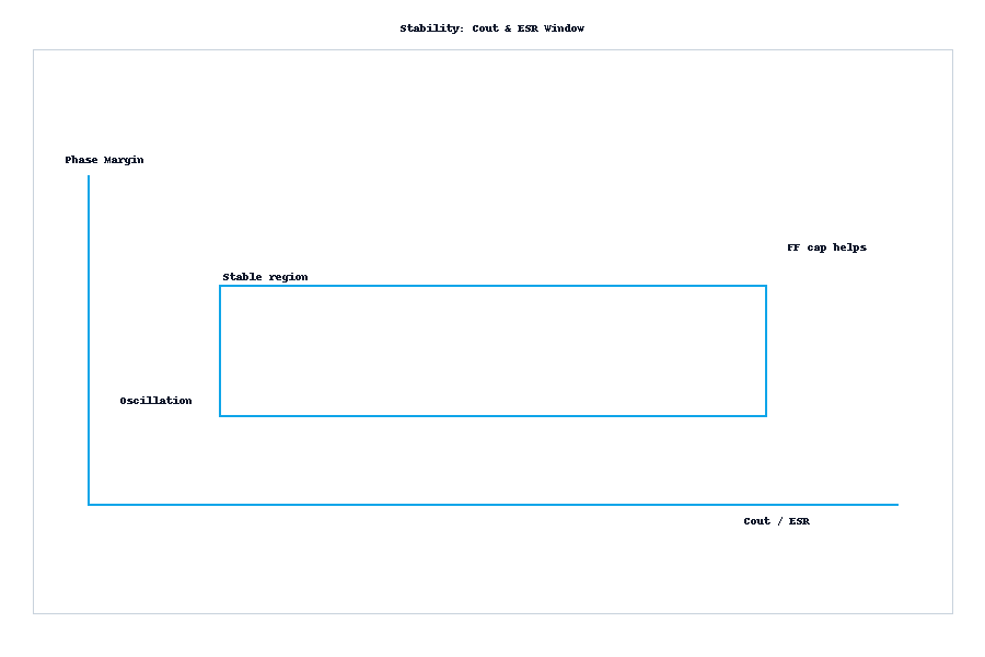
Stability Requirements
Respect the COUT/ESR window in the datasheet. Very low ESR ceramics may reduce phase margin; Cff can help but may cause overshoot. NR/BYP lowers noise with a soft-start penalty.Reference formulas
Pdiss = (Vin − Vout) × IloadΔV ≈ ΔI × ESR + ΔI × (Δt / C)Integrated Noise (µVrms) = sqrt( ∫ Sv(f) df ) (specify bandwidth)Internal Architecture & Operation
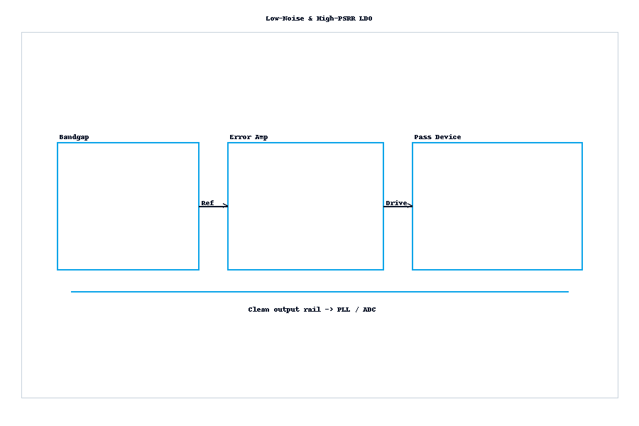
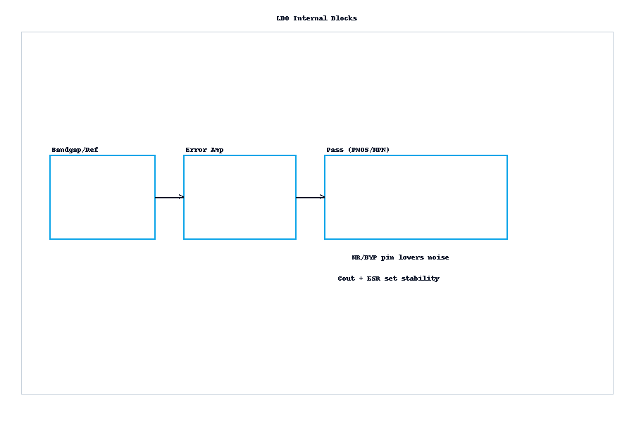
A low-noise, high-PSRR LDO is defined by its reference, error amplifier, pass device, and output network—their interactions set noise, PSRR, stability, and startup behavior.
Bandgap / Reference
Sets Vref and contributes directly to output noise unless filtered via NR/BYP. Typical approach uses a low-pass network to attenuate 1/f and wideband reference noise.Error Amplifier
Dominates low-frequency PSRR via loop gain and sets DC accuracy with offset and bias current. Its input noise is amplified by the loop and appears at VOUT.Pass Device (PMOS / NMOS / NPN)
Controls headroom and high-frequency behavior. Device transconductance and output pole location shape both transient and PSRR beyond the loop bandwidth.Feedback & Output Network
Divider resistance and tempco affect accuracy and noise; COUT and ESR/ESL set poles/zeros and phase margin. Feed-forward capacitor Cff improves step response but may increase overshoot.Pass device trade-offs
Final behavior depends on headroom, loop bandwidth, and output network placement.
NR / BYP pin
Adds a low-pass on the reference path to reduce 1/f and wideband noise. Typical values:
10–100 nF. Larger capacitance → lower noise but longer soft-start
(roughly τ ≈ RNR · CNR).
Output network & stability
COUT and ESR/ESL define poles/zeros and phase margin. Very low ESR ceramics may reduce margin; respect the datasheet stability window. Cff can improve transient response but may increase overshoot.
Noise: 1/f, Wideband, and µVrms Calculation
Separate low-frequency 1/f noise from wideband noise, disclose the measurement bandwidth, and quantify NR/BYP benefits—then your µVrms numbers become comparable and actionable.
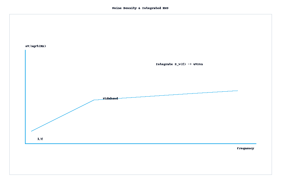
1/f noise (low frequency)
Dominates near DC; impacts audio floor and sensor drift. Filtering the reference via NR/BYP reduces how much of this region appears at VOUT.Wideband noise (mid/high frequency)
Sets integrated noise over the stated bandwidth. If density is approximately flat atS0,
then wideband only Vrms ≈ S0 · √(f2 − f1).
NR / BYP contribution
A simple RC on the reference path forms a low-pass: larger CNR (typ. 10–100 nF)
lowers noise but extends soft-start. Choose based on rail timing and inrush limits.
Bandwidth disclosure is mandatory
Always state the integration bandwidth when quoting µVrms (e.g., 10 Hz–100 kHz or
1 kHz–100 kHz). Numbers are not comparable across different BW.
How to compute integrated noise
- Pick the bandwidth: f1 to f2 (e.g., 10 Hz–100 kHz).
- From the density curve, obtain
Sv(f)across that band. - Integrate:
Vrms = √( ∫f1f2 Sv(f) df ). - Verify the instrument’s RMS detector/window and probe/grounding setup.
Measurement pitfalls
- Scope/Analyzer RMS detector and FFT windowing affect readings.
- AC coupling cutoff can remove true low-frequency content.
- Long probe ground leads inject noise; use the shortest return.
- Isolate digital rails to avoid coupling into the analog measurement.
Typical targets
- PLL / Clock rails: < 10–20 µVrms (declare bandwidth).
- High-end audio / precision AFE: strive even lower, with bandwidth disclosed.
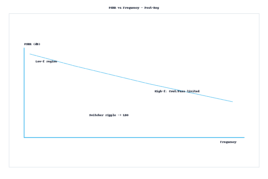
PSRR vs Frequency & Post-Regulation
PSRR is loop-gain dominated at low frequencies and pass-device/output-network limited at high frequencies; post-regulation after a switcher helps, but within realistic bounds.
Low-frequency region (loop-gain limited)
The error amplifier’s open-loop gain and reference filtering dominate LF PSRR. NR/BYP mostly helps here by reducing reference noise that the loop can’t fully reject.Mid/High-frequency region (device/network limited)
Above the loop bandwidth, the pass device transconductance and the output network (COUT, ESR/ESL, PCB/package parasitics) shape PSRR. Placement and return paths matter.Post-reg with a switching converter
Topology: Switching → RC/Bead → LDO. In the 100 kHz–2 MHz band, expect a ~15–35 dB cleanup depending on headroom, layout, and load. Treat it as meaningful but finite—not a broadband miracle.
Improve PSRR at high frequency
- Increase headroom; avoid running near dropout.
- Minimize loop area; place COUT close; ensure a tight return path.
- Use a small HF capacitor in parallel (e.g., 10–100 nF) to extend HF decoupling.
- Consider bead + RC before the LDO to pre-attenuate switching ripple.
- Shield high di/dt loops; keep FB/NR traces quiet and short.
- Validate across load states and temperature; don’t rely on one curve.
Stability: Output Capacitor, ESR, and Feed-Forward
Respect the datasheet’s COUT/ESR window, place capacitors correctly, and use Cff when needed—then verify with step-response instead of complex injections.
COUT / ESR window
Very low ESR ceramics can reduce phase margin by shifting zeros; stability holds only within the datasheet’s stated window (COUT, ESR, load, temperature). Start within that window and validate across corners.Quick guidance for capacitors
- Begin with the vendor’s recommended COUT and ESR range.
- Parallel bulk + small HF caps; place them at the pins with a tight return.
- Account for DC bias derating of ceramics; check room-to-cold ESR shifts.
- Keep FB/NR traces short and shielded from switching nets.
Feed-forward capacitor (Cff)
OUT→FB feed-forward can add a zero that improves phase margin and step response. Trade-offs include overshoot and potential peaking under some loads. Decide using a checklist: load step size/frequency, overshoot budget, target bandwidth, and datasheet examples.
Phase margin via step response
- Underdamped (ringing, overshoot): low margin → reduce loop gain near crossover or adjust COUT/ESR/Cff.
- Critically damped: healthy margin; verify across load and temperature.
- Overdamped (slow): stable but sluggish → consider Cff or more headroom if response is too slow.
- Test at min/typ/max load and across Vin to expose edge cases.
Quick estimate remains useful: ΔV ≈ ΔI × ESR + ΔI × (Δt / C).
Dropout, Iq & Light-Load Efficiency
Less headroom worsens PSRR and transient recovery while raising dissipation; ultra-low Iq often trades bandwidth for efficiency—plan for light-load artifacts.
PSRR near dropout
As headroom shrinks, pass-device gm and loop gain drop, degrading high-frequency PSRR and LF rejection.Transient margin shrinks
Lower loop gain and limited control range lengthen recovery; overshoot/undershoot grow under the same load step.Thermal stress rises
Estimate withPdiss = (Vin − Vout) × Iload; verify worst-case ambient and copper area.
Light-load noise / “hiss-burp” mitigation
| Problem | Likely cause | Fix |
|---|---|---|
| Audible hiss / bursty ripple | Burst/skip behavior at very low load | Add minimum load (resistor) or RC bleed |
| Oscillation at near-zero load | COUT/ESR outside stable window | Match datasheet C/ESR; consider small HF cap |
| Unexpected HF spikes | Poor layout / long return / probe loop | Tighten placement; use short ground spring |
Quick checks
Pdiss = (Vin − Vout) × Iload→ verify thermal rise vs RθJA and copper area.- Headroom ≥ dropout@Imax + margin (improves PSRR & recovery).
- Enforce minimum load if the part exhibits burst/skip artifacts at µA loads.
Transient Response, Soft-Start & Pre-Bias
Size ESR and C from a quick estimate, then validate with real load steps; soft-start tames inrush/overshoot, and pre-bias behavior must be confirmed for sensitive rails.
Transient quick estimate
ΔV ≈ ΔI × ESR + ΔI × (Δt / C)
— the first term is the immediate ESR step; the second is capacitive sag during the loop’s response time.
Reduce ΔV by lowering ESR, increasing C, and improving loop bandwidth/headroom.
Design checklist
- Define step magnitude/frequency and allowable overshoot/undershoot.
- Select COUT/ESR and optional Cff to meet recovery time and ΔV targets.
- Verify across min/typ/max load and Vin; include temperature corners.
Soft-start (SS)
SS limits inrush and overshoot. With NR/BYP, larger CNR reduces noise but extends start time. Consider power-good/sequence requirements; for complex rails, see the Power Sequencer sibling page.
Pre-bias start & reverse behavior
- Confirm whether the LDO sinks or ignores a pre-biased VOUT at startup.
- Avoid back-discharge into sensitive loads: check discharge FET/bleeder and consider diode isolation.
- For ADC/AFE/PLL rails, ensure no reverse path and verify ramp monotonicity.
Test method tips
- Use a fast electronic load to apply well-defined ΔI steps.
- Bandwidth-limit probes and use the shortest ground spring.
- Capture both the ESR step and the recovery to steady state.
Layout, Grounding & EMI Mitigation
Clean rails come from clean geometry: star returns, tight loops, short quiet sense lines, and properly placed beads/RC—then measure with discipline.
Star / single-point returns
Partition analog and digital grounds; route high-current returns away from sensitive nodes. Keep the LDO loop local and avoid sharing high-di/dt paths.AGND / DGND & Kelvin sense
Use AGND/DGND regions with a single tie at the quiet point. Sense VOUT with Kelvin routing at the load (or at LDO pins) to remove IR drops from feedback.Sensitive nets (NR/BYP, FB, Ref)
Keep these traces short, direct, and away from switching nodes, clocks, and hot/inductive areas. Guard/shield where needed; avoid running parallel to noisy nets.- Place NR/BYP capacitor right at the pin; shortest return to AGND.
- Route FB as a quiet sense line; avoid via stubs and plane splits.
- Do not cross high-di/dt loops; if crossing is unavoidable, cross orthogonally.
Close the loop with COUT
Place the primary COUT directly between LDO OUT and GND pins to minimize loop area. Add a small HF capacitor (e.g., 10–100 nF) close to pins to extend HF decoupling.- Avoid long thin necks between LDO and COUT.
- Use multiple vias for ground return near the capacitor pad.
- Respect the C/ESR stability window (see Stability).
Ferrite bead & RC filters
For switcher-to-LDO chains, place bead+RC before the LDO to pre-attenuate ripple. Check the bead’s impedance vs frequency; avoid creating sharp resonances with COUT and trace inductance.- Typical starting points: bead 30–120 Ω @ 100 MHz, C = 0.1–1 µF (verify with the actual spectrum).
- Add damping (e.g., small series R or parallel R across C) if peaking is observed.
- Use wideband beads for multi-harmonic ripple; place close to the LDO input pin.
Probing & measurement
Measure what the circuit sees—not the probe loop.- Use the shortest ground spring; avoid long alligator ground leads.
- Bandwidth-limit the scope (e.g., 20/100 MHz) to reduce aliasing of HF noise.
- Use AC coupling when inspecting small ripple atop DC; disclose BW and coupling in reports.
- Document test point, load state, and ambient; replicate across corners.
EMI quick wins
- Shrink high-di/dt loops; keep switch-node copper minimal and shielded.
- Prefer 45°/arc routing to sharp right angles on sensitive nets.
- Stitch ground vias around noisy areas (“via fence”).
- Route clocks and switch nodes orthogonal to analog sense lines.
- Separate power and signal return paths until the single-tie point.
Protections & Reliability
Know how the LDO protects itself—and your system—under abnormal conditions; size thermal headroom and define recovery behavior for production extremes.
Over-current protection (OCP)
Modes differ and impact restarts:- Constant-current: clamps at ILIM; can run hot.
- Foldback: current reduces with VOUT drop → lower heat.
- Hiccup: periodic retry lowers average dissipation.
- Latch-off: requires power cycle or EN toggle to recover.
UVLO & OTP
- UVLO prevents half-on operation at low input voltage; define thresholds vs sequencing.
- OTP shuts down at high junction temperature; recovery includes hysteresis—avoid thermal chatter.
Short-circuit, reverse & thermal behavior
- Short-circuit: identify protection mode; estimate heat with
Pdiss ≈ (Vin × ILIM)until the foldback/hiccup engages. - Reverse connection / back-drive: check reverse current spec; add diode or series R if the load can drive VOUT.
- Thermal shutdown: note TSD and hysteresis; ensure airflow/copper area to prevent oscillatory thermal cycling.
Thermal design & derating
Use Pdiss = (Vin − Vout) × Iload with the package’s RθJA to estimate temperature rise; verify worst-case ambient and duty. Increase copper area, add vias to internal planes, and consider airflow.
- Validate at process/voltage/temperature extremes and under batch worst-case loading.
- Include derating for long-term reliability; monitor case temperature vs ambient.
- Ensure protections don’t interact badly with system sequencing or retries.
Compliance & manufacturability tips
- Define ESD/surge limits and clamp strategy at the input.
- Specify PG/EN pull strategy and recovery timing after faults.
- Document fault triggers and pass/fail criteria for production testing.
Application Recipes
Copy-ready setups for common rails. Each recipe lists targets, a recommended BOM, and notes. Validate with Stability, PSRR, Noise and Transient sections.
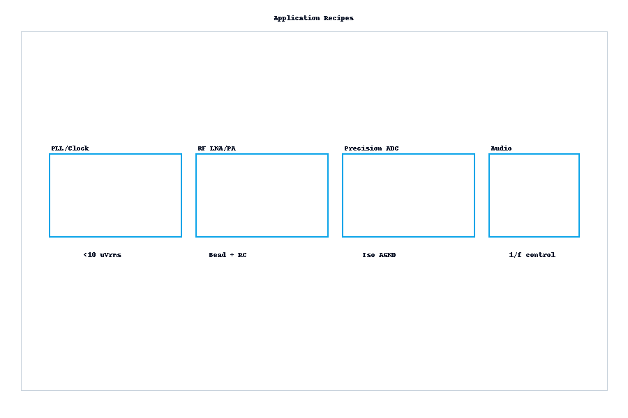
PLL / Clock Rail
- Recommended: NR =
10–100 nF; COUT =10–22 µF(+ 0.1 µF HF); pre-LDO bead+RC. - Notes: Put the detailed reference design on the sibling page Voltage Reference.
RF LNA / PA Bias
- Recommended: pre-LDO Bead → RC; COUT = bulk + mid + HF in parallel.
- Notes: For PA, watch transient droop and thermal rise during bursts.
Precision ADC / AFE
- Recommended: LDO supply + dedicated reference; COUT =
10–22 µF(+ 0.1 µF); consider Cff. - Notes: Evaluate clock jitter vs supply noise interaction (see Clock/PLL).
High-End Audio (DAC / Preamp / Headphone)
- Recommended: low-1/f LDO; use Cff judiciously; enforce clean AGND routing.
- Notes: Front-end/headphone stages are extremely sensitive to LF noise.
Tuning knobs
- Headroom: stay away from dropout to improve HF PSRR and step recovery.
- COUT/ESR: keep within the stability window; tune for target overshoot/settling.
- CNR (BYP): more noise reduction ↔ longer soft-start; verify timing.
- Bead+RC: select by spectrum and bead impedance; add damping if peaking occurs.
Validation checklist
- Noise: state integration bandwidth (e.g., 10 Hz–100 kHz).
- PSRR: record Vin/Vout/Load/COUT/temp/frequency points.
- Transient: ΔI, Δt, ΔV and recovery time; pre-bias and soft-start.
- Thermals:
Pdiss = (Vin − Vout) × Iload, RθJA, airflow and copper area. - Light-load: minimum load/RC bleed; check for hiss/burst artifacts.
Common pitfalls
- Treating device PSRR@1 MHz as system-level guarantee.
- Comparing µVrms without declaring bandwidth.
- Ignoring headroom and C/ESR stability window.
- No testing at light-load, pre-bias, and high-temperature corners.
Troubleshooting (Problem → Cause → Action)
Quick self-check
- Declare measurement bandwidth/integration window for µVrms noise.
- Use the shortest ground spring on probes; avoid long ground leads.
- Keep sense lines (NR/BYP, FB, Ref) away from switching nodes and clocks.
- Verify headroom: don’t operate near dropout during critical tests.
- Ensure COUT/ESR is inside the datasheet stability window.
- Check for too-light load; add a minimum load or RC bleed if needed.
| Problem | Likely cause | Action |
|---|---|---|
| Noise above target | Wrong integration bandwidth; long probe ground; digital coupling | Fix method (declare BW, AC-coupling, bandwidth-limit); add NR/BYP; add/retune bead+RC. |
| PSRR shortfall | Near dropout; COUT/ESL mismatch; parasitic routing | Increase headroom; change capacitors/parallel a small HF cap; tighten placement/return. |
| Oscillation / “hiss” | C/ESR outside window; load too light; Cff selection | Return to stability window; add minimum load/RC bleed; retune Cff. |
| Excessive overshoot | Cff too large; insufficient loop bandwidth | Reduce Cff; increase COUT; add headroom/select higher-bandwidth part. |
| High temperature rise | High Pdiss; high RθJA; poor airflow/copper | Lower (Vin−Vout) or load; improve heatsinking (copper/vias/airflow); choose larger package. |
FAQs
Click a question to expand.
Why does LDO PSRR fall at high frequency? How much can post-reg add?
How to choose NR/BYP capacitor? What startup delay will it add?
How to keep a ceramic COUT-only design stable?
How much dropout margin is “safe”? What does it do to PSRR/transients?
How do I measure µVrms output noise correctly?
When should I add a feed-forward capacitor (Cff)? Any downsides?
Can one LDO feed both analog and digital loads? How to isolate?
Place the ferrite bead before or after the LDO? How to choose impedance?
How to fix light-load “hiss/burp” behavior?
Will a pre-biased output back-discharge my load on startup?
Top priorities for Audio vs RF/PLL recipes?
How to thermally assess a 200–300 mA small package?
Pdiss = (Vin − Vout) × Iload, then estimate rise with package RθJA and your board stackup.
Add copper/vias/airflow and validate at hot ambient with batch-worst loads.
Probe and ground-loop errors make ripple look worse—what to do?
Why don’t my PSRR measurements match the datasheet curve?
Multi-rail systems: cascade or split rails?
Resources & RFQ
Download ready-to-use PDFs and contact us for a fast BOM review or pin-compatible options.
Low-Noise LDO Selection Worksheet
Capture Vout, Imax, noise/PSRR targets, dropout headroom, Iq, COUT/ESR window, NR/BYP, and thermal/packaging to shortlist parts fast.
PSRR & Noise Quick Rules
Ten field-proven rules for post-reg with switchers, realistic HF-PSRR expectations, and µVrms measurement caveats (bandwidth, window, probing).
LDO Bring-Up Checklist
Power-up order, measurement setup, transient/stability/thermal validation steps, and a ready-to-print record sheet for lab use.
We use your BOM solely for power-rail evaluation and recommendations. NDAs can be arranged upon request. All suggestions must be verified against the datasheet and bench validation.