
Boost & Buck-Boost Controller — Control, Compensation, and Design Flow
This page focuses on the controller layer for boost and buck-boost converters: control methods, Type-II/III compensation, power-stage matching, start-up/protections, and EMI/layout—with a practical selection and design flow. It does not cover buck controllers, multiphase/IMVP/load-line topics, PMBus/telemetry, integrated power modules, or charging/BMS (links below).
What This Page Covers
We cover boost and buck-boost controllers from an engineering perspective: control methods (voltage/current-mode, peak/valley sensing, slope compensation), loop compensation (Type-II/III), power-stage pairing (inductor, diode/synchronous FET, output capacitors), start-up and fault handling, and EMI/layout—plus selection criteria and a practical design flow.
To avoid duplication with sibling pages, this page does not cover buck-only topics, multiphase/IMVP/load-line, PMBus/telemetry, integrated power modules, or charging/BMS. Please use the links below for those areas.
Prefer a top-down view? Return to the PMIC Hub for terminology alignment and cross-page navigation.
Boost Family Topologies — Choose by VIN/VOUT Relation & Ripple Path
Pick a topology by how VIN and VOUT relate, where the ripple current flows, and what magnetics and EMI constraints you can accept. This section stays at the controller + power-stage pairing level—device lists live on regulator/module pages.
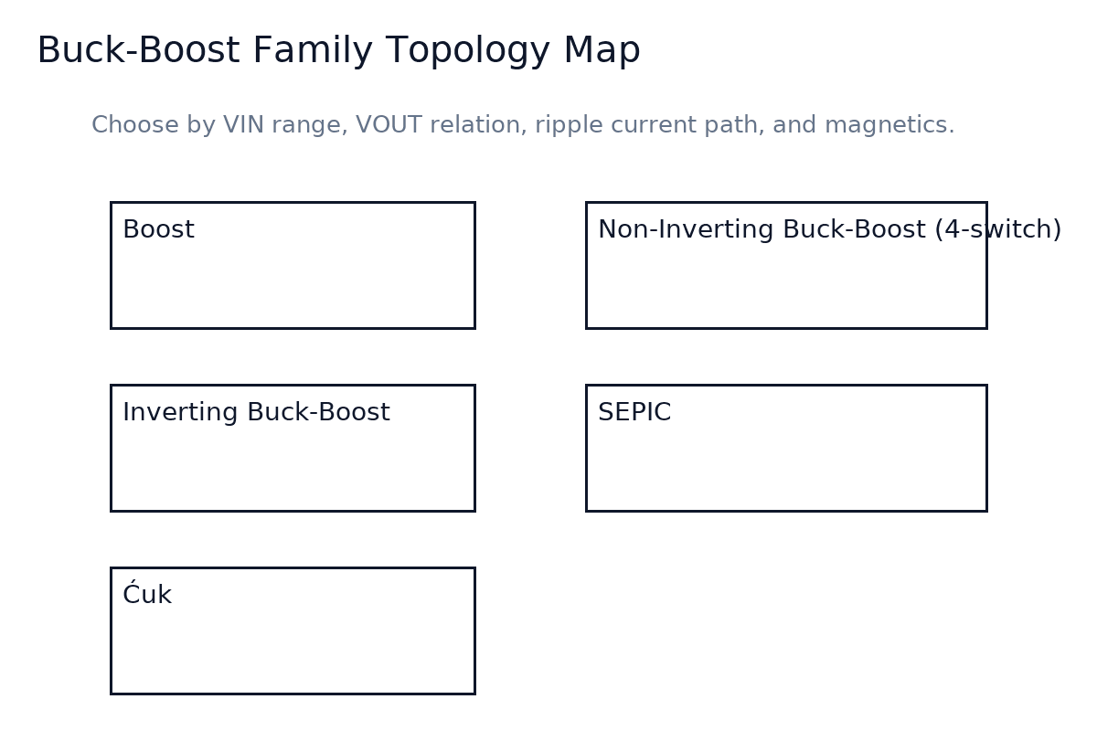
Pure Boost (Step-Up)
- When to choose: VOUT > VIN without traversing VIN≈VOUT; cost/size sensitive.
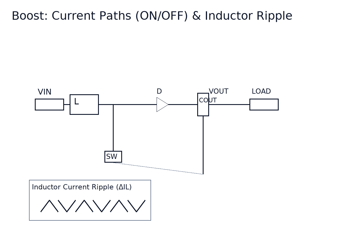
- Duty & ripple: D ≈ 1 − (VIN·η)/VOUT; size L so ΔIL ≈ 20–40% of IOUT.
- Rectifier options: diode (simplicity) vs synchronous FET (efficiency, light-load behavior).
- Reverse conduction: plan SW node clamp/sync-FET off-window to avoid back-feed.
- EMI path: hot loop around SW → rectifier/FET → COUT → GND; snubber as needed.
Non-Inverting 4-Switch Buck-Boost
- When to choose: seamless output across VIN<VOUT and VIN>VOUT (e.g., 12↔24 V automotive, variable buses).
- Control partitioning: consistent loop behavior through buck/boost regions; careful dead-time and transition damping.
- Trade-offs: more gate drivers, higher drive loss, tighter timing and layout requirements.
- Note: region transitions shift poles/zeros; limit fc accordingly (details in Control section).
Inverting Buck-Boost (Negative Rail)
- When to choose: generating a negative rail for analog/audio/op-amp bias.
- Stress profile: asymmetric switch/inductor currents; plan return path vs system ground.
- Stability & protection: sense and compensation bandwidth on negative output; align OVP reference.
SEPIC / Ćuk (Brief)
- When to choose: input traverses and/or input-to-output DC isolation (SEPIC coupling capacitor).
- Magnetics: two inductors or a coupled inductor; Ćuk can yield low output ripple with different switch stress/EMI profile.
- Boundary: where efficiency/power density is paramount and your controller supports 4-switch, prefer non-inverting buck-boost; reserve SEPIC/Ćuk for special constraints.
If your constraints point to a fully integrated solution rather than a controller + discrete power stage, see the separate Power Modules page.
Control Methods — The Stability Logic Behind Good Behavior
A boost/buck-boost controller’s stability hinges on the plant (LC, ESR zero, RHPZ) and how you sense/control current. Use this section to decide between voltage-mode vs current-mode, peak vs valley sensing, and to quantify the slope-compensation you must inject.
Voltage-Mode vs Current-Mode
- Boost (CCM) has an RHPZ: it reduces phase, so crossover fc must be limited; practically keep fc ≤ 1/10 fSW and within about 1/5–1/10 of fRHPZ.
- Voltage-mode: high design freedom; sensitive to power-stage drift; no inherent slope ramp.
- Current-mode: effectively single-pole control; compensation is more direct; peak/valley sensing choice matters.
Peak vs Valley Current Sensing
- Peak: natural OCP integration; sensitive to SW spikes and noise → needs front-end filtering/blanking.
- Valley: often calmer for light-load/burst modes; more sensitive to timing and minimum on-time constraints.
- Implementation: Rsense/DCR sensing, CS-amp bandwidth, sample-and-hold timing, blanking window and RC.
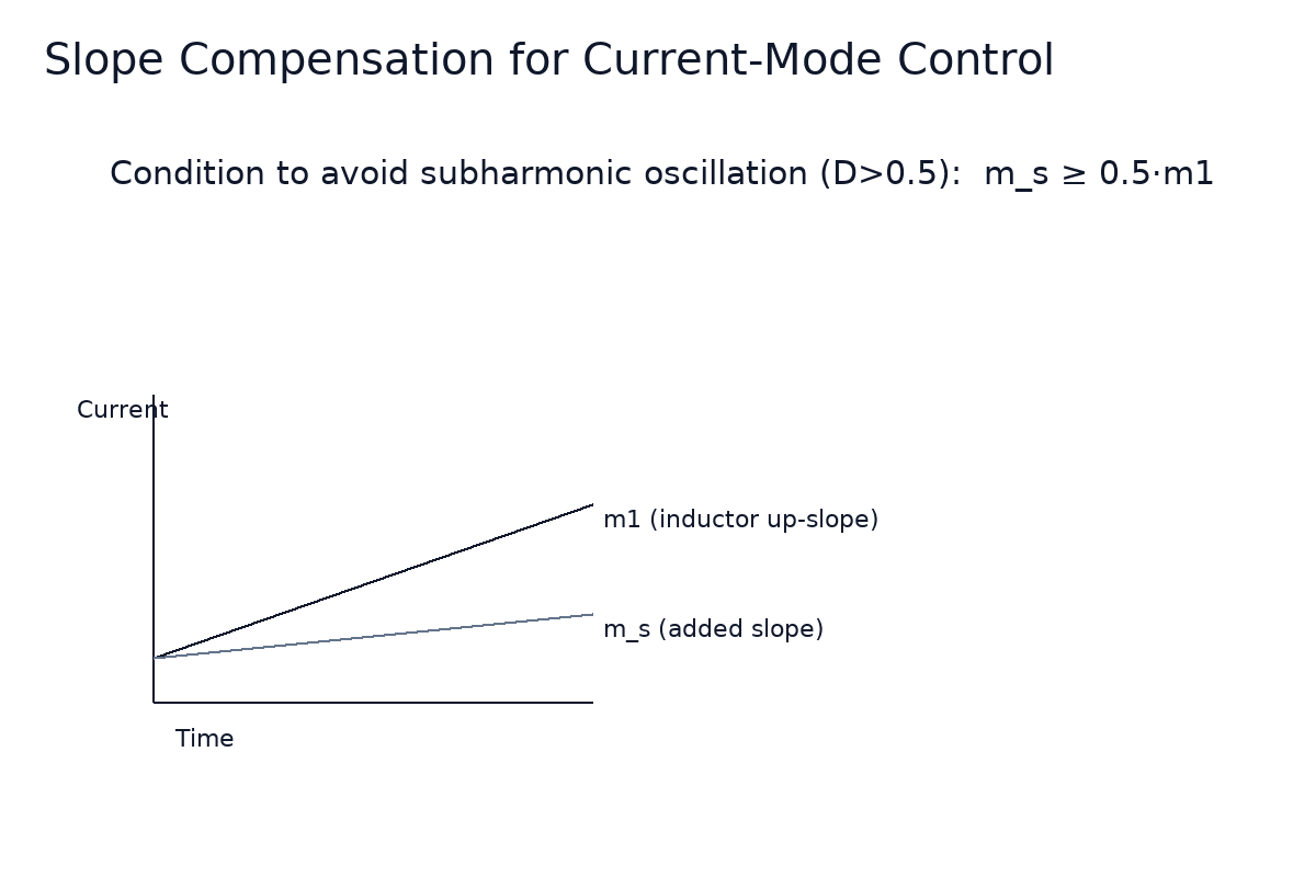
Slope Compensation (Suppress Subharmonic Oscillation)
When duty D > 0.5, inject enough ramp such that ms ≥ 0.5·m1, where m1 is the inductor up-slope and ms is the injected slope (as current or CS-voltage). Align the injection path with the sampling timing (COMP-ramp or CS-ramp) to keep loop math consistent.
Ready to translate this into zero/pole placement and Bode verification? Continue to Loop Compensation (Type-II/III) in the next section.
First-Pass Power-Stage Sizing — Practical Numbers for Boost/Buck-Boost
Duty (Boost):
D ≈ 1 − (VIN · η) / VOUT
Inductor (first estimate):
Lmin = (VIN · D) / (ΔIL · fSW)
, with
ΔIL ≈ 20–40% · IOUT
Switch Devices
- Margins: VDS, VRRM, IF with transient headroom.
- FET trade: RDS(on) ↔ Qg; package θJA; gate-drive peak current.
- Diode (async): low Qrr/trr to reduce ringing and heat.
- Sync rectification: efficiency & light-load behavior; manage reverse-conduction window.
Output Capacitors
- ESR zero: place relative to LC double pole; shape ripple & transient response.
- Ripple bucket: share ripple between ΔIL and C/ESR; validate at min-VIN/max-IOUT.
- Derating: MLCC DC-bias & temperature; consider MLCC + bulk mix.
Inductor & Quick Thermals
- Isat & losses: set ΔIL; check copper vs core at fSW.
- Shielded cores to tame EMI; consider DCR for current sensing.
- Fast thermal sanity: θJA budget + copper area; verify hotspots across ambient range.
Capture your first-pass numbers in the worksheet: Power_Stage_Sizing_Worksheet.pdf.
Loop Compensation — Type-II / Type-III for Boost & Buck-Boost
The plant is an LC double pole with an ESR zero; in boost CCM a right-half-plane zero (RHPZ) reduces phase and caps crossover. Design for healthy margins first, then refine with Bode and load-step measurements.
Targets
- Crossover: fc ≈ fSW/10 (a practical ceiling for most designs).
- Phase margin: ≥ 50–60° across VIN/IOUT corners and region transitions.
- Boost CCM note: keep fc below roughly 1/5–1/10 of fRHPZ.
Zero/Pole Placement
- Type-II: place z1/z2 near the LC double pole; use p1 near the origin to lift low-frequency gain.
- Type-III: add p2 above fc and use the extra zero/pole to shape steeper plants, e.g., 4-switch buck-boost.
- Transitions: keep a consistent fc and margin across buck/boost regions; avoid aggressive tuning near VIN≈VOUT.
Verification & Pitfalls
- Bode: inject at COMP or the loop injection node; verify magnitude & phase across VIN/IOUT corners.
- Load-step: correlate undershoot/overshoot and damping to phase margin.
- COMP gotchas: RC tolerances, leakage, and layout parasitics moving intended poles/zeros.

Need the sensing and slope context? See Control Methods above; for large-signal behavior, continue to Start-Up & Transient.
Start-Up & Transient — Soft-Start, Pre-Bias, Overshoot & Large-Signal Events
This section turns controller features into practical behavior during start-up and large load steps: soft-start/inrush, pre-bias start-up (no discharge), overshoot control in boost, and what valley current limit, minimum on-time, and AAM/PSM do to your transient response and audible/EMI profile.
Soft-Start & Inrush
- Map the ramp: soft-start slope sets inductor current rise and COUT charge current—your first inrush limiter.
- Fault windows: ensure OCP/OVP/UVLO thresholds and blanking windows don’t mis-trip during the ramp.
- Coordination: when upstream inrush control (hot-swap/eFuse) exists, align soft-start timing to avoid contention.
Pre-Bias Start-Up (Do Not Discharge VOUT)
- Goal: if VOUT is already charged, never force a discharge or negative dip at start-up.
- Controller actions: early synchronous-FET off window, soft-start reference clamped to the sensed pre-bias, controlled ramp takeover.
- Common mistake: pulling VOUT down before ramping causes audible clicks and downstream resets.
Overshoot Control in Boost
- Sources: too-steep soft-start reference, error-amp saturation, min on/off-time limits.
- Mitigations: gentler soft-start, COMP clamp/bleed path, load-feedforward, output clamp/snubber (RC/TVS) as needed.
Large-Signal Load Steps
- Valley current limit: dictates recovery time and undershoot on step-up loads; size margin for worst-case.
- Minimum on-time: with high VIN/light load/high fSW produces ripple plateaus/jitter—consider frequency and slope choices.
- AAM/PSM trade: quieter light-load modes increase ripple and may slow transients; choose “silence-first” vs “transient-first.”
Protection — Controller Features vs System-Level eFuse/Hot-Swap
Separate controller-level protections (fast, local) from system-level protection (inrush shaping, isolation, and rugged short handling). Use this section to choose modes (hiccup/auto-retry/latch) and to know when to hand off to an eFuse or hot-swap stage.
Controller-Level Protections
- OCP / ILIM / cycle-by-cycle: peak vs valley limit interactions; slope compensation influences effective threshold.
- UVLO / OVP / OTP: set windows and hysteresis; prevent false trips during start-up/soft-start.
- Fault handling: choose hiccup (cool-down safety), auto-retry (availability), or latch (serviceable isolation).
System-Level Protections (eFuse/Hot-Swap)
- Why: controlled inrush for large C or long cables, robust short-to-VIN/GND handling, downstream fault isolation.
- Interface: coordinate PG/FAULT logic and power-good delays; align soft-start with upstream dv/dt.
- Reliability: current-limit slew, short-circuit shutdown, and OTP help reduce upstream supply disturbance.
Hand-Off Criteria
- Large output capacitance or long leads requiring shaped inrush → use eFuse/hot-swap.
- Short-to-battery or short-to-ground stress cases → use eFuse with fast limit and thermal cutback.
- Need fault isolation and diagnostics (current telemetry, event logging) → system-level device.
For controlled inrush and robust short-circuit protection, see our eFuse & Protection ICs page.
EMI & Layout — Start with the Hot Loop
Tame emissions and ringing by optimizing the hot loop, routing sensitive sense lines correctly, and choosing devices that behave well at high dV/dt and dI/dt. Use this section as a practical checklist during layout review.
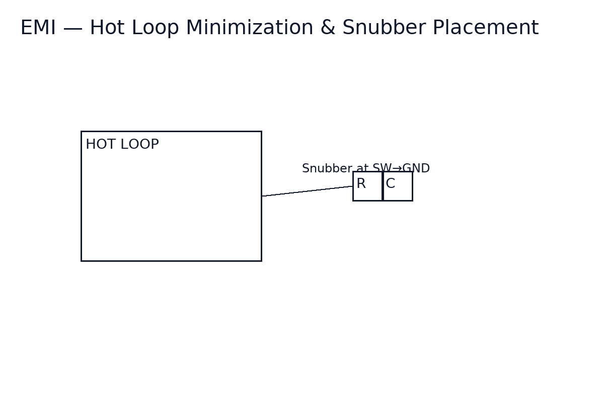
Hot Loop Minimization
- Shrink the loop SW → rectifier/synchronous FET → COUT → GND; keep return paths tight and over a solid ground plane.
- Shield sensitive nodes (FB/CS/COMP) and keep them away from the SW copper and gate-drive traces.
- Place the snubber close to the SW node; stray inductance weakens damping and shifts ringing frequency.
Sensing & Ground Partition
- Use Kelvin sensing for CS/ILIM; front-end RC/blanking must remove spikes without erasing useful slope.
- Partition AGND/PGND and converge at a star point; separate small-signal returns from power currents.
- Route current-sense and feedback lines away from high dV/dt edges; avoid vias in the critical sense loops.
Device Choices & Ringing
- Diode reverse recovery (Qrr/trr) shapes ringing; sync FET timing also matters.
- RC snubber tunes the problematic band; balance damping vs. extra loss by measuring at worst-case corners.
- Shielded inductors help reduce radiated fields and coupling into sense traces.
With the layout discipline in place, close the project loop using the 10-step design flow below.
Design Flow — Ten Steps from Specs to Sign-Off
Use this printable checklist to move from requirements to a validated, production-ready design. Each step links back to decisions covered earlier on this page.
- Specs: VIN/VOUT/IOUT, efficiency, ripple, ambient/thermal limits.
- Topology & Mode: Boost / non-inverting 4-switch / inverting / SEPIC / Ćuk.
- fSW & ΔIL: set frequency and inductor ripple target.
- Magnetics: inductor size/material/Isat and loss split.
- Switch Devices: FET/diode and gate-drive capability.
- Compensation & fc: Type-II/III, crossover and phase margin goal.
- Start-Up & Protections: soft-start, pre-bias, OCP/UVLO/OVP/OTP.
- EMI & Layout Review: hot loop, ground partition, snubber.
- Prototype Build: fixtures, probing plan, measurement points.
- Measure → Iterate → Freeze: Bode, large-signal transient, thermal validation.
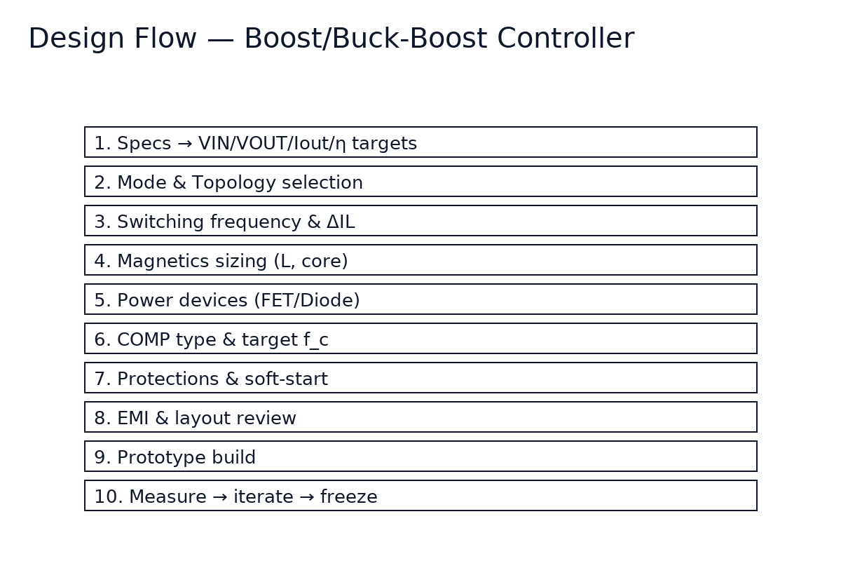
Download the printable checklist: Boost_Buck-Boost_Design_Flow_Checklist.pdf.
Need the bigger picture? Return to the PMIC Hub for glossary alignment and cross-page navigation.
Controller Selection — Compare by Fields, Not by Part Lists
Use the following decision fields to shortlist a boost/buck-boost controller for your design. Keep overlap with regulator/module pages to a minimum by staying at the parameter level.
VIN Range / VOUT Capability
- True 4-switch buck-boost for seamless VIN≈VOUT crossover.
- Boost-only when VOUT ≫ VIN and no crossover is required.
- Check absolute ratings and operating corners (cold crank, surge).
Gate-Drive Capability
- Peak source/sink current vs total Qg (including parallel FETs).
- Driver voltage (VDRV) options and bootstrap/charge-pump details.
- Single vs dual drivers; dead-time control and shoot-through immunity.
Switching Frequency Options
- Internal sync range; external clock support; spread spectrum for EMI.
- Min on-time limits at high VIN/light load; ΔIL vs efficiency.
- Light-load modes: AAM/PSM and their noise/transient trade-offs.
Compensation Method
- Internal/fixed for narrow operating ranges and simplicity.
- External Type-II/III for wide VIN/IOUT and 4-switch transitions.
- Crossover/phase margin targets across corners (see Loop Compensation).
Current Sensing
- Low-side / high-side / DCR; amplifier bandwidth and blanking windows.
- Peak vs valley detection compatibility with your protection scheme.
- Calibration and temp drift (especially with DCR sensing).
Protections & Soft-Start
- ILIM strategy, cycle-by-cycle limit, hiccup/auto-retry/latch.
- UVLO/OVP/OTP ranges; pre-bias start-up behavior.
- Overshoot control hooks (COMP clamp/bleed, load feedforward).
Package & Thermal
- θJA targets and copper area guidance; thermal pad layout.
- Pinout that supports hot loop minimization and clean sense routing.
- Automotive/industrial ratings if applicable.
Map these fields to your use-case with the application cards below.
Application Cards — Map Decisions to Real Scenarios
Automotive 12 → 24 V
Spec: VIN 9–16 V (crank/surge), VOUT 24 V, IOUT 2–5 A, EMI robustness.
- Topology: non-inverting 4-switch buck-boost for seamless VIN≈VOUT crossover.
- Control/Comp: Type-III; keep consistent fc across regions; consider spread spectrum.
- Protection/EMI: UVLO/OVP/OTP; pair with eFuse for controlled inrush; minimize hot loop.
For layout discipline, see the EMI & Layout section above.
USB-PD 5 → 20 V
Spec: VIN 5–12 V, VOUT 20 V, up to 60–100 W; prioritize efficiency & overshoot control.
- Topology: synchronous Boost.
- Control/Comp: current-mode with slope compensation; fc ≤ fSW/10; pre-bias start-up.
- Protection/EMI: OVP/hiccup; account for cable IR drop; snubber at SW node.
For slope/peaking details, see Control Methods.
Audio Power Amplifier Boost
Spec: VIN ~12 V, VOUT 24–36 V; noise/“pop” suppression and clean transients.
- Topology: Boost with suitable input filtering.
- Control/Comp: manage AAM/PSM noise; COMP clamping/bleed to contain overshoot/pop.
- Protection/EMI: tuned sync-FET timing; shielded inductor; RC/TVS damping.
Tie this back to Start-Up & Transient for pop/overshoot control.
Portable 3.7 → 12 V
Spec: VIN 2.8–4.2 V (cell), VOUT 12 V; tight size/efficiency constraints.
- Topology: choose between SEPIC (input decoupling) and 4-switch (efficiency/density).
- Control/Comp: respect minimum on-time at high fSW; Type-III for bandwidth margin.
- Protection/EMI: pre-bias start-up; MLCC bias derating; thermal budget & light-load efficiency.
Cross-check with Power-Stage Sizing for ΔIL and thermal targets.
FAQs — Quick Answers with Pointers
Why is current-mode often preferred for boost/buck-boost steady-state and transients?
How do I implement slope compensation when D > 0.5 in real hardware?
How does the boost CCM RHPZ limit fc, and how high can I push it?
Peak vs valley current sensing — noise and protection trade-offs?
How to “quick-size” the RC snubber at the SW node?
How does pre-bias start-up avoid discharge and overshoot?
Inductor too small vs too large — stability and loss consequences?
Is phase margin harder in 4-switch buck-boost than in pure boost?
How do AAM/PSM light-load modes affect ripple and EMI?
How to handle minimum on-time induced output ripple/jitter?
When must I choose SEPIC/Ćuk instead of 4-switch?
Synchronous FET reverse conduction — risks and mitigations?
Resources & RFQ — Get Help, Fast
Design Flow Checklist (PDF)
Printable 10-step flow from specs to validation. Use it in design reviews and sign-off meetings.
Boost_Buck-Boost_Design_Flow_Checklist.pdfPower-Stage Sizing Worksheet (PDF)
Capture first-pass numbers: duty, inductor, device stress, and thermal notes for early prototypes.
Power_Stage_Sizing_Worksheet.pdf