
Load Switch / Ideal Diode-OR — Practical Selection & Design
Focused subpage under PMIC. Scope: high-side load switches and ideal-diode OR paths (reverse-current blocking, inrush via dV/dt, priority). Heavy short-circuit energy and hot-swap boards live on the eFuse/Hot-Swap page; multi-rail sequencing and PMBus supervision live on the Sequencer/PSM page.
Intro & Use Cases
This page covers high-side load switches and ideal-diode ORing only. For high-energy faults and hot-plug backplanes, see the eFuse / Hot-Swap page. For multi-rail timing and PMBus/telemetry, see Sequencer and PSM.
- Portable / USB-C source handover (adapter ↔ battery)
- Automotive 12 V sub-system isolation (avoid backfeed)
- Dual-supply backup with priority (master/slave, voltage-priority, GPIO override)
- Module hot-plug (limit inrush; quick discharge via QOD; reverse-current blocking)
How They Work
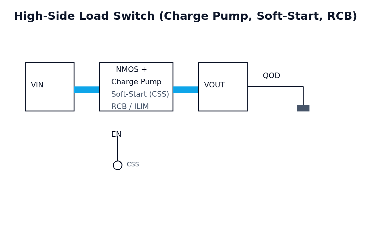
Load Switch
Core: high-side NMOS with a charge pump (gate above VIN → low RDS(on)). Key blocks: QOD (quick output discharge), RCB (reverse-current blocking), current-limit (constant/foldback/timed) plus soft-start dV/dt via CSS.
Engineering tip: over-aggressive current-limit can stall startup or brown out upstream; QOD on analog rails may need a gentler discharge.
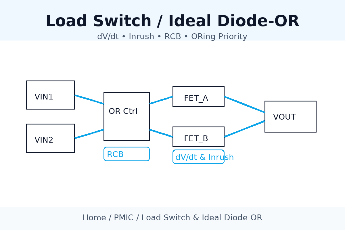
Ideal Diode-OR
Goal: millivolt-level forward drop and no backfeed during switchover. A comparator/op-amp senses source delta-V and drives MOSFETs to keep VSD ≈ a few mV. Back-to-back FETs give true bidirectional blocking; priority/hysteresis avoid flapping when sources are close.
Engineering tip: align priority policy (master/voltage/GPIO) with downstream UVLO/boot sequence to prevent reset loops.
Next up: in Key Parameters & Quick Rules, we turn inrush, conduction loss and temperature rise into quick numbers; then in Design Recipes we apply them to common current ranges.
Topologies
Choose the power-path structure first; reverse-current capability and switchover behavior depend on it.
Single FET
Lowest cost, small drop. Without RCB, it cannot block reverse current.
- Simple high-side path; minimal BOM
- Good for single-direction rails with no backfeed risk
Caution: May backfeed during power-down or reverse conditions.
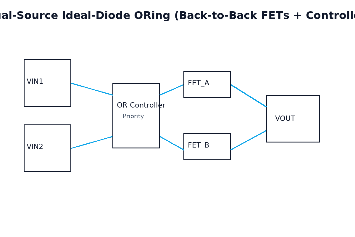
Back-to-Back FETs
Sources tied together for bidirectional blocking.
- Symmetric on/off behavior
- Best for battery/USB parallel systems and OTG
Caution: Gate drive must ensure safe, coordinated on/off.
Ideal-Diode Controller + FET
Millivolt-level forward drop, strong gate drive, and priority/hysteresis.
- Clean ORing and fast switchover
- Use when drop/thermal and policy control matter
Caution: Mis-set thresholds can cause source flapping.
Integrated Ideal-Diode
Controller + FET in one package; compact for small/medium currents.
- Small footprint, simple routing
- Great for portable or modular boards
Caution: Current and thermal headroom limited by package.
Key Parameters & Quick Rules
Evaluate these first; they drive loss, temperature rise, and switchover stability.
- RDS(on): sets conduction loss and temperature.
- I_LIMIT: constant / foldback / timed; defines overload behavior.
- dV/dt / CSS: limits inrush current during startup.
- QOD: fast discharge at turn-off; coordinate with up/downstream bleed.
- RCB: true reverse blocking (critical for battery↔USB parallel paths).
- tON / tOFF: ties into sequencing and UVLO/reset.
- VFWD / VOR: path/ORing drop; too high → droop & heat.
- IREV: max reverse current (ideal target ≈ 0).
Quick rules:
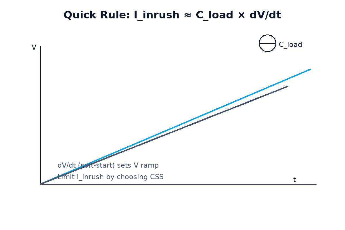
Iinrush ≈ Cload × dV/dt
PFET ≈ I² × RDS(on)
ΔT ≈ P × θJA
Worked example (5 V rail)
Target dV/dt = 2 V/ms, Cload = 220 µF → Iinrush ≈ 220e-6 × 2e3 = 0.44 A.
Steady 2 A, choose RDS(on)=20 mΩ → P ≈ 2² × 0.02 = 0.08 W.
With θJA=60 K/W → ΔT ≈ 0.08 × 60 = 4.8 K (comfortable margin).
Continue to Design Recipes for current-range playbooks and validation steps.
Design Recipes
Pick a scenario and apply the checklist. Each recipe lists a recommended topology, critical settings, a quick validation script, and common pitfalls.
≤ 2 A rails (phones / MCU / logic)
Topology: Load switch with integrated current limit (+ optional QOD). RCB depends on whether the rail is paralleled with other 5 V sources.
- Set I_LIMIT ≈ 1.2–1.5 × steady current.
- Set dV/dt via CSS to cap inrush to source capability.
- Enable QOD for digital-only loads; avoid on sensitive analog rails.
- RCB only if backfeed is possible (parallel 5 V or battery paths).
Validation script:
- Scope startup: verify ramp (dV/dt) and Iinrush within target.
- Check upstream droop/UVLO during enable.
- Turn-off with QOD: ensure no disturbance to analog references.
Pitfalls: Over-tight current limit causes restart; QOD can inject noise into ADC rails.
2–5 A board-level 5 V
Topology: Programmable current limit + back-to-back FETs + RCB; QOD enabled; CSS sets slew.
- Back-calculate dV/dt from Cload and target Iinrush.
- Choose RDS(on) for ≥ 2× Irms thermal headroom.
- Enable RCB (mandatory in parallel/OR paths).
- Use QOD but verify downstream discharge current limits.
Validation script:
- Cold/Hot start ramps; confirm Iinrush and tON.
- Short overload pulse: confirm limit mode and recovery.
- Backfeed test (VOUT>VIN): confirm reverse block and gate behavior.
Pitfalls: Non-synchronous gate drive across the two FETs can create momentary stress.
Dual-supply OR / Priority
Topology: Ideal-diode controller + external FET(s) (or integrated ideal-diode) with priority/hysteresis.
- Select policy: master/slave, voltage-priority, or GPIO override.
- Add hysteresis / timers to prevent flapping near equal source voltages.
- Target VOR/VFWD for drop/thermal limits.
Validation script:
- Switchover: main→backup→main under steady and dynamic load.
- Load steps during handover: ensure no brownout/reset.
- GPIO override window: confirm debounce and dwell time.
Pitfalls: Tight thresholds with no hysteresis lead to oscillatory priority changes.
USB-C / Adapter + Battery in Parallel
Topology: Ideal-diode path + back-to-back FETs for anti-backfeed; configure directionality and thresholds for charge vs OTG.
- Enable RCB in both directions.
- Limit upstream current and set slew during OTG.
- Validate priority across protocol voltage windows.
Validation script:
- Mode switch: charge ↔ OTG; confirm direction and limits.
- Plug/unplug & power-down backfeed test.
- Large Cload inrush test vs upstream tolerance.
Pitfalls: No OTG limit or too-fast slew can drag the adapter or battery into brownout.
Before finalizing BOM, verify thermal/SOA limits under worst-case conditions (next section).
Thermal & SOA
Confirm conduction loss, junction rise, and short-pulse survivability. Thermal shutdown in a load switch is self-protection—not an eFuse-class energy handler.
Power & Junction Temperature
- PFET ≈ I² × RDS(on); use Irms for duty-cycled loads.
- ΔT ≈ P × θJA; check worst ambient and airflow.
- Keep 10–20 K thermal headroom at max load.
Short Pulses & SOA
- Check SOA curves vs pulse width, repetition, and junction temperature.
- For ideal-diode FETs, verify VDS and current limits during switchover.
- Use current limit and dV/dt to tame surge energy when needed.
Thermal Shutdown ≠ eFuse
- Load-switch thermal shutdown is self-protection, not a controlled fuse event.
- For high-energy shorts, load dump, or backplane hot-plug, use eFuse/Hot-Swap controllers.
- Consider TVS, inrush shaping, and staged turn-on for harsh transients.
If your scenario involves load dump or large-energy faults, route to the eFuse / Hot-Swap page. For BOM help, see Resources & RFQ.
Layout & EMI Tips
A practical checklist for reliable bring-up: minimize loops, place capacitors correctly, keep references clean, and provide thermal paths.
Minimize High-dI/dt Loops
- Keep VIN → FET → VOUT copper tight and short.
- Reduce hot-loop area to cut ringing and radiation.
- Route input and return in parallel where possible.
Pitfall: Long, thin high-current traces cause droop and EMI.
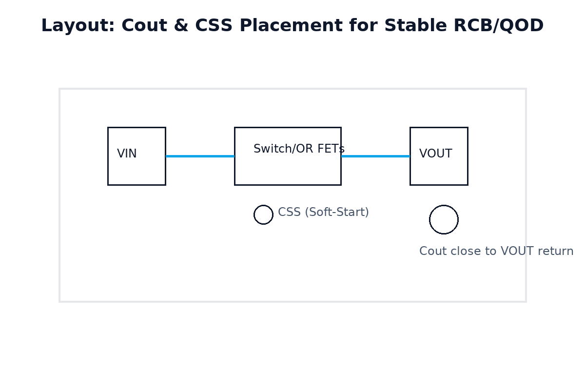
Place Capacitors Intelligently
- Put COUT close to VOUT and its return.
- Place CSS next to EN/control pin to stabilize slew.
- Use staged capacitance (low ESR/ESL parts in parallel) for large loads.
Pitfall: A remote CSS can inject noise and make dV/dt inconsistent.
Grounding & Sensing
- Use star ground or dedicated sense ground.
- Run comparator/op-amp references on a clean ground.
- Kelvin sense critical nodes for accurate thresholds.
Pitfall: High current return through reference ground causes false trips or flapping.
Thermal Paths
- Flood copper on FET pads; stitch vias to inner/other layers.
- Align hot parts with airflow; avoid thermal shadowing.
- Validate θJA with copper area and board stackup.
Pitfall: Ignoring package limits/parallel sharing invites thermal shutdown.
Brand & Series (Index)
Series-level index only (not a product page). For side-by-side matrices or pin-compatibility checks, use the downloads/consultation links on Resources & RFQ.
TI
TPS229xx (load switch), TPS212x (priority/ideal-diode control), LM73100 (ideal diode / RCB).
Covers phone/board rails to medium-current OR/priority paths.
ST
STEF, STMPS, VIPower series.
Load switches and protection-oriented paths.
NXP
NX5P (USB/5 V, with RCB/limit).
Popular in portable and interface rails.
Renesas
ISL7xxx / RAA families include load-switch / OR controllers.
Controller-centric options for ORing and protection.
onsemi
FPF, NIS (ex-Fairchild IntelliMAX).
Board-level load switches with protection variants.
Microchip
MIC20xx / MIC940xx (load switches); MCP16xx (selected ideal-diode parts).
Compact options for small/medium current paths.
Melexis
Lower relevance for this topic; when needed, consider TI / Microchip / onsemi equivalents first.
Use as a cross-check only if specific constraints apply.
Need pin-compatibility or drop-in alternatives? Head to Resources & RFQ for worksheets and help.
Selection Checklist (Copy & Paste)
Use this list to complete first-pass selection and review. Copy it into your design ticket or review doc.
- Input range (incl. absolute max).
- Peak & steady current (state Ipeak, Irms).
- Target RDS(on) (back-calc from loss & thermal).
- dV/dt / soft-start (CSS) (set from Iinrush target).
- Need RCB? (parallel/backfeed/battery paths) [tip: bidirectional block]
- Need QOD? (avoid on precision analog rails) [tip: gentle discharge]
- Current-limit mode (constant / foldback / timed) [tip: start-up margin]
- Over-temperature (shutdown & recovery thresholds).
- Package / θJA / copper (heatsinking, vias, parallel if needed).
- On/Off timing & dependencies with sibling rails (UVLO/reset coordination).
- Validation script (inrush / thermal / droop / priority handover / EMI).
FAQs
Expand a topic below. Each answer is concise (≈50 words) and links back to the most relevant section.
What’s the core difference between a load switch and an eFuse, and when must I use an eFuse?
eFuses handle high-energy faults and isolation (shorts, over-voltage, reverse, retry/latch) and suit hot-plug backplanes. Load switches focus on ramp control, inrush limiting, and modest faults. If surge energy or line inductance is significant, prefer an eFuse. See Design Recipes and Thermal & SOA.
Single FET vs back-to-back FETs for reverse-current blocking?
A single FET relies on its body diode and cannot block in both directions. Back-to-back (sources tied) FETs provide true bidirectional blocking, essential for battery/USB parallels and OTG. Gate drive must coordinate both devices. See Topologies.
How do I estimate Iinrush from Cload and dV/dt, and choose CSS?
Use Iinrush ≈ Cload × dV/dt. Pick a target Iinrush, solve for dV/dt, then map to CSS (or external slew resistor) per the datasheet. Verify upstream supply droop and UVLO margins during startup. See Key Parameters.
Can I enable QOD and RCB together? Any caveats?
Yes. QOD discharges VOUT at turn-off, and RCB blocks reverse current. For analog/precision rails, use gentle discharge or series resistance to avoid upsetting references. Confirm discharge current limits and timing. See How They Work and Layout & EMI.
Why does priority switchover “flap,” and how do I prevent it?
Flapping occurs when source voltages are too close and load transients create dips. Add hysteresis and dwell timers, or use a GPIO override window. Set clearer thresholds in the OR controller. Validate under load steps. See Design Recipes.
How do I avoid USB / 5 V backfeed between sources?
Use an ideal-diode path with RCB enabled. For OTG, define directionality and add back-to-back FETs as needed. Validate plug/unplug and power-down backfeed, plus large-C inrush versus adapter/battery limits. See Design Recipes.
Risks of too-slow vs too-fast soft-start?
Slow ramps prolong startup and can trigger UVLO or watchdog timeouts. Fast ramps raise Iinrush, EMI, and upstream droop. Balance against reset thresholds and source capability; choose CSS for a safe dV/dt and verify with scope. See Key Parameters.
Quick way to estimate FET temperature rise and when to upsize/parallel?
Compute P ≈ I²·RDS(on) and ΔT ≈ P·θJA. If ΔT nears limits at worst ambient, move to lower RDS(on), larger packages, or parallel devices with shared copper. Validate with steady-state thermals and airflow. See Thermal & SOA.
How do I verify reverse-current blocking (RCB) under VOUT > VIN?
Force VOUT > VIN and monitor IREV and VIN waveform. Check controller specs and thresholds; use back-to-back FETs if needed for true bidirectional block. Confirm behavior at temperature and during turn-off. See Key Parameters.
What noise effects can QOD/RCB introduce on analog/ADC rails?
Fast QOD can couple discharge transients into reference ground; prefer gentle or resistive discharge on precision rails. Keep comparator references on clean ground and route sense lines away from hot loops. See Layout & EMI.
How do cold-crank and load-dump in 12 V automotive constrain selection?
Check transient withstand/clamping, short-pulse SOA, and thermal protection over temperature. For severe load-dump or high-energy shorts, pair with eFuse/Hot-Swap and TVS suppression. Validate with worst-case profiles. See Thermal & SOA.
How to confirm pin-compatibility and consistent startup behavior when replacing parts?
Don’t stop at pinout—match soft-start slope, limit strategy, RCB/QOD behavior, and timing. Replicate startup/turn-off waveforms on the bench and compare thresholds and delays. Check thermal margins after the swap. See Design Recipes and Key Parameters.
Resources & RFQ
Grab the toolkit below. Need a shortlist in 48 hours? Submit your BOM. Prefer a quick inquiry? Use the form right here.
Selection Worksheet
Capture inputs, targets, and protection choices for load switch / ideal-diode OR.
PDF
application/pdf ·
ls-idor-selection-worksheet.pdf
dV/dt & Inrush Calculator
Map Cload, ramp time, and dV/dt to Iinrush; size CSS quickly.
XLSX
application/vnd.openxmlformats-officedocument.spreadsheetml.sheet ·
ls-idor-inrush-calculator.xlsx
ORing FET Sizing — Quick Guide
Pick RDS(on), check drop/thermal, and review SOA for priority ORing paths.
PDF
application/pdf ·
ls-idor-oring-fet-sizing.pdf
Bring-Up & Validation Checklist
Scope ramps, confirm inrush/RCB/QOD, and check thermal/EMI before release.
PDF
application/pdf ·
ls-idor-bringup-checklist.pdf
Related topics: eFuse / Hot-Swap · Power Sequencing · PMBus PSM