
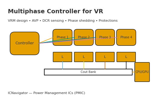
Multiphase Controller for VR (VRM)
This page focuses on engineering the multiphase VRM controller for high-current CPU/GPU/SoC rails—phase planning, current sensing, load-line/AVP tuning, compensation for transients, light-load phase shedding, and protections. With a tightly scoped structure and downloadable checklists, teams can deliver a verifiable, shippable, and mass-production-ready VR solution.
Back to Hub — PMIC
Scope & relationship. This page is a child of the PMIC hub and addresses only the control, tuning, and verification of multiphase VRM controllers for core rails. It deliberately avoids duplicating topics covered by sibling pages. Use the hub for high-level navigation and return here for controller-centric guidance.
What this page covers
- Multiphase control concepts and implementation: phase interleaving/management, current sensing and balancing, load-line (AVP) tuning, compensation and transient targets, light-load behavior, and VR-side protections.
What this page does not cover (use sibling pages instead)
- Single-phase / generic buck design → see Buck Converter IC.
- Board-level protection / hot-swap / eFuse → see eFuse & Protection ICs.
- System-level sequencing / PMBus PSM / alert aggregation → see Power Sequencer / PMBus PSM.
- MOSFET gate driving, DrMOS / Smart Power Stage packaging, loss analysis → see MOSFET Driver / DrMOS.
Definition & Use Cases
A multiphase VRM controller coordinates several parallel power stages (DrMOS/Smart Power Stage), using interleaving (phase shifting), current balancing, and loop compensation to deliver tightly regulated core voltage for high-current, fast-transient loads such as CPUs, GPUs, and ASICs.
Why multiphase instead of single-phase?
- Higher current via parallel phases with proper current sharing.
- Lower output ripple from phase interleaving and larger effective switching frequency.
- Faster transient response enabled by optimized compensation and AVP (load-line) tuning.
- Thermal spreading across multiple inductors and power stages for better hotspots control.
Where it is used
- Desktop/Server VRM — CPU Vcore/Vcache rails with steep di/dt.
- GPU / AI accelerator cards — high-current core rails, HBM/SerDes auxiliaries (controller-centric items only).
- Switch/Storage ASICs — network/IO chips demanding tight regulation under bursts.
- HPC / Edge AI — dense boards requiring efficiency, transient speed, and thermal balance.
60-second checklist
- Phase planning: current target, Fsw, interleaving, external sync need?
- Sensing: DCR vs Rsense vs SPS IMON; accuracy vs loss vs drift.
- Compensation: Type II/III, crossover bandwidth, phase margin ≥45–60°.
- AVP: droop slope (mΩ) and transient window (±mV) matched to spec.
- Protections: total/per-phase OCP, OVP/UVP/OTP and fault policy.
VR Electrical Requirements
Define the boundary conditions for the VRM controller: current profile and slew, ripple targets, efficiency & thermal budget, top-side protocol hooks (VID/SVID/AVS), rationale for load-line/AVP, and VR-side startup constraints. These inputs gate phase planning, sensing choice, compensation, and protection limits.
Current & Slew
- ILOAD,max / ILOAD,avg / ILOAD,idle (A)
- Slew (A/µs) at worst step; duty cycle of bursts
- Corner cases: VIN / T / aging / tolerance
Ripple & Regulation
- VOUT target & tolerance (±mV or %)
- Ripple limit (mVpp) at load points
- DC accuracy vs dynamic window priorities
Efficiency & Thermal
- η targets at idle / nominal / max load
- Hot-spot limit (°C) & airflow constraints
- Loss split: switching, conduction, magnetics
VID / SVID / AVS Hooks
- Interface: VID table / SVID / PMBus-AVS (concept level)
- Commandable VOUT range & step size
- Telemetry: IMON / temperature / fault flags
Why Load-Line / AVP?
A small intentional droop (Rdroop, mΩ) trades DC headroom for transient room, reducing undershoot/overshoot during fast steps. First-order check:
- ΔV ≈ Istep · Rdroop → choose Rdroop so ΔV fits the allowed window (±mV)
- Verify with compensation bandwidth and Cout ESR/ESL limits
- Calibrate IMON so AVP is consistent over temperature
Startup / Soft-Start / Black-Start
- Soft-start ramp rate vs inrush & pre-bias handling
- Black-start under short / heavy load behavior
- System-level sequencing is covered on the Power Sequencer / PMBus PSM page
Requirements Table (template)
| Parameter | Target / Spec | Notes / Corner |
|---|---|---|
| VOUT target & tolerance | — | ±mV or % |
| ILOAD,max / avg / idle (A) | — | Profile & duty |
| Slew (A/µs) & step width | — | Worst-case |
| Ripple (mVpp) | — | At load points |
| Efficiency targets (η) | — | Idle/Nom/Max |
| Thermal limit (°C) / airflow | — | Hot-spot map |
| Interface (VID/SVID/AVS) | — | Range & step |
| Load-line Rdroop (mΩ) | — | Transient window |
| Startup / soft-start ramp | — | Pre-bias, inrush |
| Telemetry (IMON/temp/fault) | — | Scale & accuracy |
Fill this table or download the worksheet in Resources & RFQ (Design Checklist / Load-line Tuning / Transient Script).
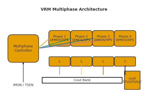
System Architecture
Overview of the signal/power path and phase management in a multiphase VRM. We outline how the controller orchestrates DrMOS/SPS stages, inductor bank, and output capacitors to feed the load; how interleaving and switching frequency are planned; when to use external sync/spread-spectrum; and how phase shedding and telemetry (IMON/TMON/TSEN) are integrated.
Power & control topology
- Controller — PWM generation, phase management, protections, telemetry interfaces.
- DrMOS / Smart Power Stage (SPS) — per-phase high/low FET + driver (gate drive details on Driver/DrMOS page).
- Inductor bank — one per phase; sets ripple & current sharing dynamics.
- COUT array — bulk + ceramic mix; defines transient and ripple window with ESR/ESL.
- Load (CPU/GPU/SoC) — VID/SVID/AVS control of set-point (concept level only).
Interleaving & FSW planning
- Phase interleaving: spread switching edges by 360°/N to reduce output ripple.
- Effective ripple frequency ≈ N × FSW (first harmonic), easing COUT requirements.
- Trade-offs: higher FSW improves transient but increases switching loss.
- Rule of thumb: target crossover ≈ (0.05–0.1) × FSW, then verify stability margins in #control.
External Sync & Spread-Spectrum (concept)
- External sync: align VRM switching with system clock to avoid beat tones/EMI collisions.
- Spread-spectrum: modulate FSW slightly to flatten EMI peaks (verify loop stability).
- Clock routing and jitter budgets belong to the system/clocking page; only concept mention here.
Phase Shedding & Telemetry
- Phase shedding: reduce active phases at light load to lift efficiency; re-add on demand.
- Hysteresis & debounce to prevent chatter; verify output ripple during transitions.
- IMON/TMON/TSEN: per-phase current & temperature feedback for balancing and protection.
- Link to #light-load for efficiency curves, to #sensing-balancing for current sharing.

Quick planning guide
- Phase count (N): meet IMAX and thermal; ensure margin for transient slew.
- Inductor L & DCR: set ripple/current sharing; mind DCR for DCR-sensing accuracy.
- COUT mix: ceramic for HF; bulk/polymer for energy; check ESR/ESL windows.
- Telemetry: calibrate IMON scale; use TMON/TSEN to limit per-phase stress.
Current Sensing & Balancing
Compare DCR sensing, Rsense shunt, and SPS/IMON telemetry; then pin down sampling windows, filtering, and inter-phase current balancing. The goal is stable accuracy over temperature with minimal loss, while keeping each phase within stress limits.
DCR Sensing (Inductor DCR)
- RC equivalence: sense V across L’s DCR via an R-C network emulating L/R time constant.
- Delay compensation: match τ = L/DCR; compensate residual phase delay in the controller.
- Temperature drift: DCR ↑ with T; require temp coefficient or calibration tables.
- Pros: no extra I²R loss; low cost. Cons: accuracy drifts; layout-sensitive.
Practical tip: keep RC sense traces short, use Kelvin to inductor pads, and place RC close to the controller pins.
Rsense Shunt
- Accuracy: well-specified tolerance and TCR; best for precise OCP/AVP enforcement.
- Loss trade-off: added I²R loss; evaluate η impact at nominal and max load.
- Differential routing: Kelvin sense across shunt; symmetrical return; avoid shared ground drops.
- Pros: high accuracy, linearity. Cons: power loss, thermal rise, BOM + area.
Choose low-inductance shunts; keep sense pair tightly coupled and away from switch node.
SPS / IMON Telemetry
- Scale: each Smart Power Stage reports current (IMON) and temperature (TMON/TSEN).
- Calibration: map IMON code → A using vendor scale; trim offset/gain at 25 °C & hot.
- Drift: verify accuracy vs T and phase stress; re-balance thresholds accordingly.
- Integration: feed IMON to controller for per-phase OCP and balancing loops.
Cross-check IMON against bench shunt during bring-up; store trims in NVM/OTP if available.
Sampling Windows & Filters
- Cycle-by-cycle sampling captures ripple and fast faults; more noise.
- Averaged sampling for AVP/telemetry; apply finite window (e.g., 4–8 cycles).
- Anti-alias: align sample instant away from SW edges; RC/DFT-style digital filters if provided.
- Latency budget: total sense→decision delay must not destabilize current share loop.
Inter-phase Current Balancing
- Algorithms: average bus share, master-slave trim, or per-phase PI adjust.
- Inductor tolerance: L/DCR spread skews share; add slow trim to equalize.
- Thermal tie-in: derate hot phases via TMON; keep ΔI between phases within spec.
- Stability: choose share-loop bandwidth ≪ voltage loop; avoid hunting with load steps.

Next: Control & Compensation Skip to: Load-Line & AVP Tuning
Control & Compensation
Choose an appropriate control mode and design a practical compensation network to meet bandwidth, stability margin, and transient targets. We keep formulas minimal here—see the PDFs in Resources for worksheets.
Voltage-Mode (VM)
- Inner power stage modeled as LC; compensation must generate adequate ripple injection / slope.
- Pros: simple loop visualization; low current sense noise sensitivity.
- Cons: load/line changes shift plant; requires robust Type III more often.
- Variants: fixed-frequency with ramp injection; some controllers add feed-forward.
Current-Mode (CM)
- Inner current loop linearizes power stage; outer voltage loop is easier to compensate.
- Pros: fast line transient, predictable plant; good with AVP.
- Cons: needs slope compensation at high duty; sense accuracy/drift matters.
- Per-phase CM in multiphase helps current sharing and OCP response.
COT / Valley / Fixed-Frequency
- COT (Constant-On-Time): excellent transient; pseudo-fixed frequency; watch EMI/ton jitter.
- Valley/Peak control: uses ripple for turn-on; ensure clean ripple injection path.
- Fixed-F: predictable EMI profile; easier sync/spread-spectrum; may need more Cout for transient.
Compensation: Type II / Type III
- Target crossover (fc): typically 0.05–0.1 × FSW; keep phase margin ≥ 45–60°.
- Type II (one zero, one pole): suitable when inner current loop is strong or plant is well-damped.
- Type III (two zeros, two poles): for voltage-mode or aggressive fc / light Cout ESR.
- Zero placement: place first zero near LC double pole; second zero to boost phase near fc.
- High-frequency pole: roll off at 1/2–1 × FSW (or RHPZ) to reduce switching residue.
- AVP coupling: when using load-line, ensure IMON/AVP path latency does not eat your phase margin.
| Scenario | Suggested Type | Notes |
|---|---|---|
| Per-phase current-mode, decent ESR | Type II | Zero @ LC; HF pole near 1/2 FSW |
| Voltage-mode, ceramic-heavy Cout | Type III | Add second zero to boost phase at fc |
| COT / Valley with AVP | Type II/III (case by case) | Mind ripple injection & AVP latency |
Transient Design Targets
- Step amplitude & edge: define Istep (A) and slew (A/µs) per #requirements.
- Undershoot/overshoot: respect window from #loadline; check droop contribution.
- Settling: time to within ±x mV; ring-down at acceptable Q.
- Multi-step: test consecutive bursts and load pattern to expose chatter.
Bode vs Load-Step — Who checks what?
- Bode: crossover fc, phase margin, gain margin; verifies small-signal stability.
- Load-step: large-signal transient—undershoot, overshoot, settling, waveform shape.
- PRBS/noise injection: optional; validates loop model vs real hardware.
- Capture across VIN/temperature/corners; reference Transient Test Script.
Practical Tips
- Keep AVP/IMON path latency small; add compensation pole only after validating margin.
- Do not place fc too close to ESR zero or RHPZ (if present).
- When phases are shed, confirm the loop remains stable in minimal-phase mode.
- Store final R/C values and fc, margin, and captures in the project checklist.
Load-Line & AVP Tuning
Move from a target droop to window calculation and finally to bench calibration. We set an equivalent Rdroop (mΩ), account for static/dynamic terms, map it to the spec’d transient window, and close the loop with IMON calibration and temperature compensation.
Set Rdroop (mΩ): logic
- Spec window: allowed undershoot/overshoot (±mV) at the defined Istep & slew.
- First-order tie: ΔVAVP ≈ Istep · Rdroop.
- Budget split: Window = AVP share + Cout/loop share; leave margin for loop & ESR/ESL.
- Cornering: verify at VIN, T (cold/hot), and tolerance of L/ESR/ESL.
Static vs Dynamic components
- Static droop: DC slope across load; eases undershoot but reduces DC headroom.
- Dynamic term: loop/Cout response adds/subtracts from AVP; validate by load-step.
- IMON coupling: AVP path may use IMON; ensure latency < loop phase-margin budget.
IMON Closed-Loop Calibration
- Baseline: measure I via precision shunt; read IMON code/voltage.
- Fit: derive gain/offset (25 °C) → program trims / NVM if available.
- Check: repeat at multiple loads; verify AVP slope from IMON agrees with target.
- Corner: re-check at hot/cold; update temp coefficient table if supported.
Tip: keep AVP/IMON filter constant small enough to follow load-step statistics but large enough to reject SW ripple.
Temperature Drift Correction
- DCR rise with temperature skews sensed current → apparent AVP error。
- Apply gain vs T trim or table; bind to TMON/TSEN per-phase temperature.
- Re-verify transient window at hot to ensure undershoot budget remains valid。
AVP Tuning Worksheet (inline)
| Item | Value / Target | Notes |
|---|---|---|
| Allowed transient window (±mV) | — | Spec limit |
| Istep (A) & slew (A/µs) | — | From #requirements |
| Rdroop target (mΩ) | — | ΔV ≈ Istep·Rdroop |
| IMON gain / offset | — | 25 °C trims |
| Temperature coefficient | — | Hot/cold correction |
| Measured ΔV @ step (mV) | — | Scope result |
| Pass/Fail vs window | — | OK / adjust |
Download the detailed worksheet: VRM_Loadline_Tuning_Worksheet.pdf (with formula notes and recording pages).
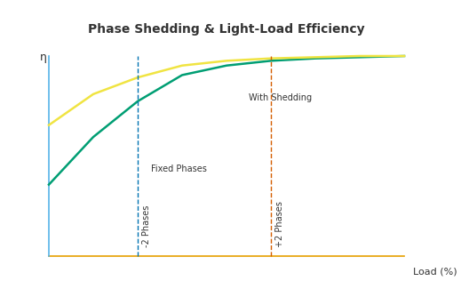
Light-Load & Phase Shedding
Balance efficiency with ripple and stability when the rail enters light load. Define robust phase-shedding thresholds, a smooth re-add strategy, and understand how PSM (pulse-skip / burst / hiccup) modes alter transient behavior and acoustic/EMI profiles.
Shedding Thresholds
- Ished down: below this per-phase current, drop 1–n phases to cut switching loss.
- Hysteresis: set Iadd up ≥ (Ished + margin) to avoid chatter.
- Debounce: time-based filtering (e.g., 5–50 ms) against load dithering.
- Min phases: verify loop stability and ripple in the 1-phase (or 2-phase) mode.
Re-Add Strategy
- Step-wise ramp-in: add phases one at a time with ramped duty/ILIMIT to prevent output dip.
- Thermal bias: prefer cooler phases first (TMON) to equalize aging and hotspot stress.
- Soft-sync: align to interleaving grid before enabling the phase’s gate drive.
- Fault gating: skip bad phases (IMON/OT warn) until cleared.
PSM Modes & Effects
- Pulse-skip: reduces average FSW; watch ripple growth and potential audible tones.
- Burst / hysteretic: clusters of pulses; excellent η but larger low-freq ripple.
- Hiccup: fault-recovery style; for real faults only, not normal light load.
- EMI/Acoustics: consider spread-spectrum; damp magnetics to avoid whine.
Impact on Transient & Loop
- Mode hop testing: step load across Ished/Iadd and check undershoot/overshoot.
- Loop stability: confirm phase margin in minimal-phase mode (#control).
- Telemetry tie-in: IMON filtering must not hide a needed phase-add event.
- Ripple window: ensure mVpp at light load remains within spec.
Practical Checklist
- Define Ished/Iadd and debounce; verify no chatter across 0–100% load patterns.
- Measure mVpp ripple and audible noise in minimal-phase & PSM modes.
- Validate thermal balance after shedding with TMON; cap per-phase ΔI.
- Log events and trims in the project checklist (#checklist); retest over VIN/T corners.
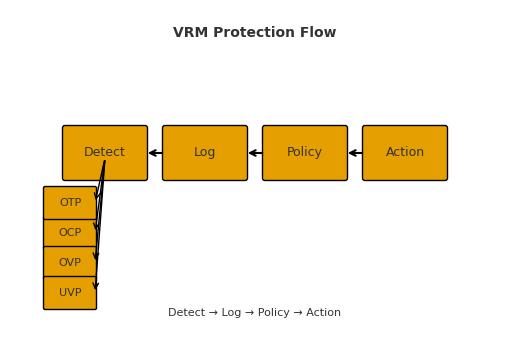
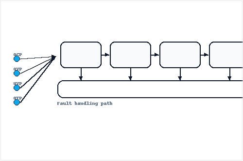
Protections & Fault Response
Define a VR-side protection matrix and a deterministic fault-handling path. This section focuses on controller-level thresholds and actions; system-wide alert aggregation and sequencing are handled elsewhere.
Protection Matrix (VR-side)
- OCP: total rail OCP + per-phase OCP (detect current imbalance / phase fault).
- OVP / UVP: fast latched OVP to protect silicon; UVP with blanking during transients.
- OTP: controller and per-phase (TMON/TSEN) limits; apply derating / phase gating.
- Black-start / short-start: controlled ramp, ILIMIT clamp, fast shutdown on hard short.
Fault → Log → Policy → Action
- Fault detect: threshold compare with debounce / blanking (ms) to reject chatter.
- Log: timestamp, rail ID, phase ID, IMON/TMON snapshot for RMA.
- Policy: retry count, cool-down, phase-disable vs whole-rail shutdown, latch or auto-rearm.
- Action: soft-off, hiccup, phase isolation, or latched off; signal PG low as needed.
Thresholds & Actions (template)
| Function | Threshold / Spec | Debounce / Blanking | Policy | Action |
|---|---|---|---|---|
| OCP (Total) | IOCP,total = — A | — ms | Retry ×N, cool-down — ms | Hiccup / soft-off / latch |
| OCP (Per-phase) | IOCP,phase = — A | — ms | Isolate bad phase; continue if safe | Phase-off; re-add after cool-down |
| OVP (Rail) | VOVP = — V | Fast (µs) | Latch preferred | Immediate shutdown |
| UVP (Rail) | VUVP = — V | Blanking — ms (ignore load step) | Retry with limited ILIMIT | Soft-off or hiccup |
| OTP (Per-phase / Controller) | THOT = — °C / TWARN = — °C | — ms | Derate first; then shut if sustained | Phase-gate / rail off |
| Black-start / Short-start | ILIMIT during ramp = — A | Fast short detect (µs) | 1–N retries, progressive back-off | Immediate shutdown / latch |
Practical Notes
- Set per-phase OCP slightly above balanced share; catch runaway phases early.
- Use TMON to derate hot phases; prevent thermal ratcheting during shedding (#light-load).
- Keep UVP blanking aligned with transient windows to avoid false trips during load steps.
- Record all trips in a fault log; export with the project checklist (#checklist).
Layout, Thermal & EMI Tips
A VRM’s performance lives or dies on sense routing, return paths, and thermal/EMI discipline. Use the following checklists to keep the controller stable, the phases balanced, and the board quiet.
Sense & Reference Networks
- Differential sensing back to the load pads; keep pair tightly coupled.
- Kelvin connections for Rsense/DCR nodes; avoid shared high-current copper.
- Single-point ground for reference/compensation; split analog/digital grounds and join at star point.
- Place RC sense (DCR emulation) and COMP parts close to the controller pins.
- Guard traces / keep-outs near SW nodes to cut ripple injection.
Inductor & COUT Arrays
- Shortest high-current loop: FET → L → COUT → FET; minimize loop area.
- Distribute COUT (ceramic near load; bulk at bank) to meet HF/LF needs.
- Use via arrays (staggered) for heat/current; avoid bottleneck neck-downs.
- Orient inductors consistently to align magnetic fields; avoid coupling hot spots.
- Check return path continuity on every layer; no unintended slots.
Thermal & EMI Discipline
- Map hotspots (IR/thermocouples) at worst VIN/I; add copper pours & vias under DrMOS/SPS.
- Align airflow with inductor/DrMOS rows; leave keepout for heatsinks/ducts.
- Control edge rates if supported; consider spread-spectrum for EMI peaks.
- Prevent slot antennas: no long ground splits crossing high di/dt loops.
- Use proper probes/bandwidth for measurements; avoid ground leads forming loops.
Redline Rules (copy & paste)
Diff sense from load pads, tightly coupled, away from SW; Kelvin at Rsense/DCR nodes.
Analog COMP/REF returns meet digital ground at a single star—no shared high-current copper.
Minimize FET–L–COUT–FET loop; place ceramics at the phase output and near the load.
Use dense via arrays under DrMOS/SPS and COUT grounds; avoid necked traces.
Do not route high di/dt returns over split planes/slots; preserve continuous ground under power loops.
Tame switch edges if available; enable spread-spectrum after verifying loop stability.
Use ground spring tips; bandwidth ≥100 MHz for transient; avoid long ground leads.
Balance phase currents using TMON; derate or reorder phase add-in when hotspots rise.
Layout/EMI Mini Checklist
| Item | Status | Notes |
|---|---|---|
| Diff sense & Kelvin done | ☐ | — |
| COMP/REF star ground | ☐ | — |
| Shortest power loop achieved | ☐ | — |
| Via arrays under DrMOS/COUT | ☐ | — |
| No ground slots under returns | ☐ | — |
| EMI spread/edge-rate validated | ☐ | — |
| Probe method & BW checked | ☐ | — |
Design Flow & Checklist
A pragmatic, end-to-end flow for multiphase VRM delivery—from requirements through validation to production lock. Use the inline checklist and the downloadable worksheets to maintain a closed verification loop.
- Requirements → capture VOUT, IMAX, slew (A/µs), ripple (mVpp), η/thermal, VID/SVID/AVS (#requirements).
- Phase & FSW planning → choose N, interleaving, sync/SS options (#architecture).
- L/C selection → size inductor ripple & DCR; mix COUT (ceramic/bulk) for transient/ripple.
- Sensing → pick DCR / Rsense / SPS-IMON; layout for accuracy (#sensing-balancing).
- Compensation → Type II/III; fc=0.05–0.1·FSW, phase margin ≥45–60° (#control).
- Load-line (AVP) → set Rdroop vs transient window; plan IMON calibration (#loadline).
- Protections → OCP(total/phase), OVP/UVP/OTP, black-start policy (#protections).
- Light-load strategy → shedding thresholds, debounce, re-add path, PSM checks (#light-load).
- Thermal/EMI → hotspot map, airflow, spread/edge-rate; redline layout review (#layout).
- Production lock → freeze trims (IMON/AVP), OTP/NVM image, version & sign-off package.
Bring-up & Validation
- Load-step script: undershoot/overshoot & settling; corners for VIN/T/loads.
- Bode/PRBS: confirm fc, phase/gain margins; pre/post AVP trim.
- Thermal/power map: IMON/TMON logging; per-phase ΔI and hotspot control.
- Batch consistency: sample multiple boards; re-test trims & window compliance.
Lock & Release Artifacts
- OTP/NVM image & checksum; trim tables (IMON gain/offset, AVP).
- Final limits: OCP/OVP/UVP/OTP, Ished/Iadd, debounce/blanking.
- Measurement captures: scope/Bode PDFs; thermal IR shots; CSV logs.
- Versioned checklist signed by EE/PE/QA.
Project Checklist (inline)
| Item | Owner | Status | Notes / Link |
|---|---|---|---|
| Requirements sheet (spec window, slew) | — | ☐ | #requirements |
| Phase/FSW plan | — | ☐ | #architecture |
| L/C selection & models | — | ☐ | Datasheets/SPICE |
| Sensing choice + layout constraints | — | ☐ | #sensing-balancing |
| Compensation (fc, margins) | — | ☐ | #control |
| AVP Rdroop target & IMON trims | — | ☐ | #loadline |
| Protections matrix & policies | — | ☐ | #protections |
| Shedding thresholds & tests | — | ☐ | #light-load |
| Thermal/EMI review & redlines | — | ☐ | #layout |
| Production lock (OTP/NVM, limits) | — | ☐ | Checklist signed |
Downloads
- VRM_Multiphase_Design_Checklist.pdf — master checklist to track flow, limits, trims, and sign-offs.
- VRM_Transient_Test_Script.pdf — step-load procedure, capture settings, and pass/fail criteria.
Selection Guide
Use these selection dimensions to shortlist a multiphase VRM controller. We avoid model dumping; instead, evaluate capabilities, compatibility, protections, and physical constraints against your requirements.
Controller Capabilities
- Max phases & phase mapping modes (dual-rail? N+M?).
- Sync / external clock support; spread-spectrum options.
- FSW range and resolution (set-point steps).
- VID / SVID / AVS handling; VOUT step size; slew control.
- Telemetry granularity: IMON resolution, per-phase TMON/TSEN, fault flags.
Power-Stage Compatibility
- Gate/drive signaling levels & timing compatibility with DrMOS/SPS vendors.
- IMON/TMON interface format (voltage, PWM code, I²C/PMBus hooks).
- OCP sense method match (DCR/Rsense/SPS-IMON) and calibration support.
- See MOSFET Driver / DrMOS for package loss & gate-drive details.
Protections, Package & Footprint
- Protection granularity: per-phase OCP? per-phase OTP? fast OVP latch?
- Policy options: retry counts, cool-down timers, phase isolation.
- Package & thermal: θJA/θJC, exposed pad, layout keepouts.
- Footprint: pin pitch, OTP/NVM configuration pins, test headers.
- Board-level protection lives in eFuse & Supervisors.
Shortlist Matrix (fill with 2–4 candidates)
| Dimension | Candidate A | Candidate B | Candidate C |
|---|---|---|---|
| Max phases / rails | — | — | — |
| FSW range / sync / SS | — | — | — |
| VID/SVID/AVS & Vout step | — | — | — |
| Telemetry (IMON/TMON) granularity | — | — | — |
| Sense method (DCR/Rsense/SPS) | — | — | — |
| Per-phase OCP/OTP & policies | — | — | — |
| Package / footprint / θ | — | — | — |
| Notes / risks | — | — | — |
FAQs
Concise, engineer-focused answers. Each item links back to the relevant section.
What’s the core difference between multiphase and single-phase buck?
How do I rough-estimate phase count and switching frequency?
DCR vs. sense-resistor: how should I choose?
Does phase shedding at light load impact stability?
How do I set the droop slope and transient window?
Type II or Type III compensation—how to decide?
How should I set per-phase OCP thresholds?
When do I need external clock sync or spread-spectrum?
Why is my ripple higher than expected—and how to debug?
What does Bode prove vs. a load-step test?
How do I calibrate AVP using IMON?
How do I troubleshoot inter-phase current imbalance?
How do VR12/VR13/IMVP relate to this page?
Resources & RFQ
Download the worksheets and scripts (open in a new tab), then submit your BOM for a fast review. We’ll keep these assets updated as the guide evolves.
VRM Multiphase Design Checklist
Master checklist for requirements → validation → production lock.
Download PDFLoad-Line / AVP Tuning Worksheet
Compute Rdroop, allocate transient window, and record IMON trims.
Download PDFTransient Test Script
Step-load procedure, capture settings, and pass/fail criteria.
Download PDFReady to move? Send us your design.
Tip: include target phases, FSW, AVP slope, sensing method, and any platform VID/telemetry constraints for a faster turnaround.