
Smart Power Stage (DrMOS) — Architecture, Specs, and Integration
A Smart Power Stage (DrMOS) integrates the high-side MOSFET, low-side MOSFET, and gate driver in one package, cutting parasitics and loop length to improve multiphase VRM efficiency, thermal control, and consistency.
This page focuses on how to select and integrate DrMOS—from internal blocks and key specs to layout/thermal, protections, and a pin-compatible migration path.
The goal is to finish a 48-hour minimal loop: load → phases → SPS pick → layout/thermal checks → bring-up.

What Is a Smart Power Stage (DrMOS)?
A Smart Power Stage (DrMOS) integrates the high-side MOSFET, low-side MOSFET, and the gate driver in a single package to minimize parasitics and loop length, boosting multiphase VRM efficiency and thermal consistency.
- Parasitics & loop: Package-level routing reduces Ls/Coss/Qg impact versus discrete FETs + driver.
- Consistency: Factory-matched timing/dead-time improves phase-to-phase symmetry and current sharing.
- Board area: Smaller footprint and shorter gate/boot traces simplify power stage placement.
- Design effort: Fewer parts and fewer layout pitfalls enable faster bring-up.
- Thermals & reliability: Defined exposed-pad heat path and built-in protections (UVLO/OTP/OC) reduce corner-case risk.
When a Discrete Power Stage Can Still Win
- Very high VIN or unusual voltage classes where SPS options are limited.
- Ultra cost-down designs where discrete FETs are significantly cheaper.
- Exotic thermal/mechanical constraints that require custom split locations.
Control-loop compensation and IMVP policy are covered on the Multiphase Controller page. Driver theory and gate timing details live on the Gate Driver ICs page. For the full category overview, see the PMIC hub.
Need pin-compatible options for your board? Jump to Resources & RFQ.
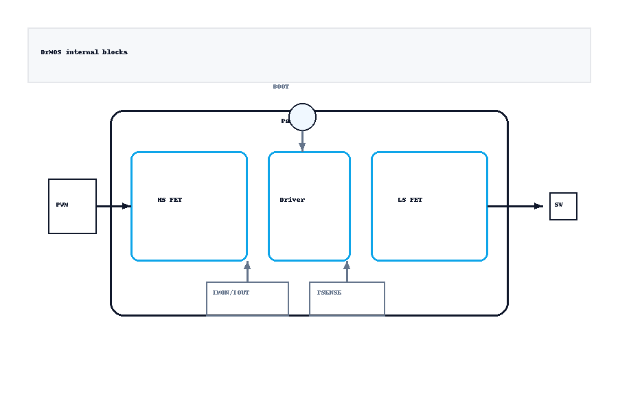
Inside a DrMOS: Architecture & Signals
A DrMOS/Smart Power Stage integrates the following internal blocks and pins for a compact, low-parasitic power stage:
- Power FETs: High-side MOSFET (HS), Low-side MOSFET (LS) tied to the SW node.
- Gate Driver: Level-shift + timing control with dead-time management.
- Bootstrap: BOOT cap/diode path for HS gate drive.
- Telemetry: IMON/IOUT (current sense/export), TSENSE (case/inner temperature sense).
- Status/Protections: PG/FAULT signaling; built-in UVLO/OTP/OC (details in §7).
- Control/Power Pins: PWM logic (3.3/5 V, polarity per datasheet), VDRV/VCC for driver, VIN for HS FET.
Typical Signal Flow
- PWM logic from the controller enters the internal gate driver.
- The driver commutates HS/LS MOSFETs with managed dead-time, creating the switching SW node.
- IMON/IOUT and TSENSE export telemetry back to the controller for current limiting, thermal management, and logging.
- PG/FAULT conveys package-level status to system logic (aggregation covered in the PMBus/PSM page).
Pin/Interface Checklist (Quick Verify)
- PWM: logic level (3.3/5 V), polarity/tri-state behavior, input threshold.
- VDRV/VCC & VIN: operating range, UVLO, decoupling placement.
- IMON/TSENSE: scaling/offset, reference routing (Kelvin), filter recommendations.
- PG/FAULT: active polarity, open-drain vs push-pull, controller pin mapping.
Need a drop-in replacement? Get pin-compatible options.
Key Electrical Specs That Really Matter
These parameters directly determine losses, efficiency, EMI, thermal headroom, and the quality of telemetry/limits. Use the checklist below to connect each spec to an engineering outcome.
| Parameter | What it affects | Engineering note |
|---|---|---|
| RDS(on) (HS/LS) | Conduction loss, phase temperature, efficiency at mid–high load | Prioritize LS RDS(on) at high current; HS impacts during on-time and transient peaks. |
| Qg, Qrr, Coss/Qoss, SW slew | Switching loss, EMI, ringing, light/medium-load efficiency | Lower charge helps high Fsw; manage slew to balance EMI vs loss (snubber/boot resistor as needed). |
| tON/tOFF & Dead-Time | Shoot-through risk, diode conduction, reverse recovery stress, light-load efficiency | Too short → shoot-through; too long → body-diode penalty. Verify at hot/cold corners. |
| IMON/IOUT accuracy (with temp drift), TSENSE path | Telemetry fidelity, current limit loop, thermal throttling | Check scaling/offset and drift; route Kelvin, filter per datasheet, calibrate at 3 points. |
| VIN / VDRV (VCC) / PWM level | Operating range, logic compatibility, margin to UVLO | Confirm PWM level (3.3/5 V) and polarity/tri-state; place decoupling caps tight to pins. |
| UVLO threshold, OC/OT limits & tolerances | Startup robustness, fault immunity, protection repeatability | Ensure thresholds align with system rails; note ± tolerance to avoid nuisance trips. |
| Package, ΘJA/ΘJC, exposed pad | Heat path, hotspot temperature, allowed current per phase | Size via farm under pad; reserve copper area; coordinate inductor airflow path. |
Quick Engineering Checks
- Run two operating points: hi-I/low-Fsw and mid-I/high-Fsw to bound losses.
- Validate dead-time at hot/cold corners; inspect SW ringing and diode conduction time.
- Calibrate IMON offset/slope across temperature; log with the bring-up checklist.
- Confirm UVLO/OC/OT margins versus rail tolerance and ambient/airflow scenarios.
Want a short list tuned to your Iout and Fsw? Get pin-compatible options.
Selection Guide: From Load to Part Number
Follow this seven-step path to move from load requirements to a concrete DrMOS part number, then shortlist pin-compatible alternates for efficiency, cost, and supply resilience.
-
Load current & rails.
Define Iout (nominal/peak), rail count, target Vout, ambient, airflow.
-
Initial phase count (experience window).
Use the ranges below as a quick start; refine after Step 3.
Iout (nominal) Typical phases Notes ≤ 40 A 1–3 Low density; prioritize cost and ΘJA. 40–120 A 3–6 Mainstream CPU/GPU rails; balance efficiency vs BOM. ≥ 120 A 6–12 High density; watch thermals, airflow, pad copper. -
Per-phase current & thermal budget.
Compute Iphase ≈ Iout / Nphases × derating (e.g., 0.8 for margin). Check ΘJA/ΘJC, pad copper, and via array against your ambient/airflow.
-
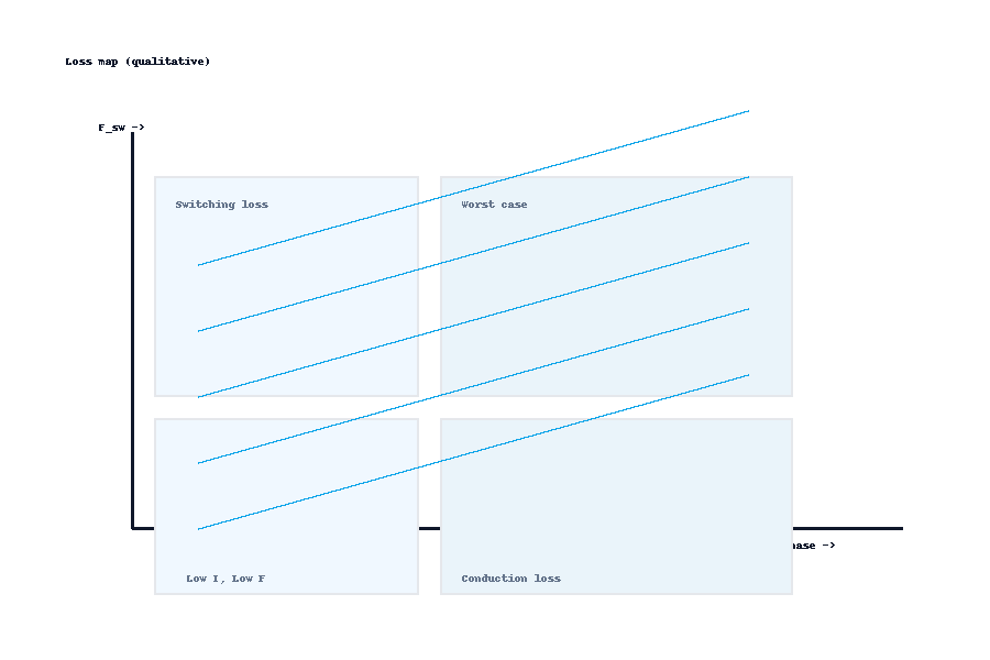
Frequency window.
Select an Fsw range (e.g., 300–600 kHz) based on transient needs and magnetics. Higher Fsw improves response but increases switching loss (see §3 loss map).
-
Quick loss estimate.
Use vendor calculators or a simplified split: Pcond from RDS(on) at Iphase, plus Psw from Qg/Qoss/Coss at chosen Fsw; verify dead-time penalties. Aim for temperature headroom at worst-case (hot, high line, high load).
-
Package / footprint constraints.
Confirm exposed-pad size, pin-1, PWM polarity level (3.3/5 V), IMON/TSENSE pins, and nearby inductor envelope. Keep a consistent land pattern to enable drop-in alternates.
-
Pin-compatible shortlist (3 choose 1).
Build a three-option set: efficiency-first, cost-first, supply-robust. Verify: PWM level & polarity, tri-state behavior, UVLO/OC/OT thresholds, IMON/TSENSE scaling, and package pad map.
Use the Worksheet (Fast Fill)
Download the structured worksheet to capture the key inputs and compare three pin-compatible candidates side-by-side.
Fields included
- Iout, Nphases, Iphase, Fsw
- RDS(on), Qg, ΘJA
- AUX note (ambient, airflow, constraints)
- Candidate PN / Package / PWM polarity & level / Compatible controllers
⬇️ Download: SPS_Selection_Worksheet.pdf
Want us to fill it for you and return a shortlist? Submit your BOM (48h).
PWM & Compatibility Nuances
Verify these items before committing a DrMOS to a given controller. Keep this list focused on interface and logic behavior; loop compensation and IMVP policy live on the Multiphase Controller page.
PWM Signal (Logic Interface)
- Level: Controller PWM output at 3.3 V or 5 V; DrMOS input absolute max, VIH/VIL thresholds, input hysteresis.
- Polarity: Normal vs inverted; ensure consistency across all phases (mixed polarity is a common bring-up pitfall).
- Tri-state behavior: What voltage = high-Z detect? How is HS/LS forced (both off) during tri-state? Startup/shutdown default.
- Timing limits: Min pulse width, max PWM frequency, input rise/fall time; controller’s dither/jitter still recognized as valid PWM.
- Bias domains: If the controller IO is 3.3 V but DrMOS expects 5 V (or vice-versa), confirm tolerance or add level shifting.
EN / PG / FAULT Interactions
- EN pin: Active level and threshold; sequencing with controller VR_EN; any soft-start dependency.
- PG (power-good): Polarity (active-high/low), driver type (open-drain vs push-pull), required pull-up voltage, debounce/blanking time.
- FAULT: Latch vs auto-retry, clear method (EN toggle / PWM tri-state / power cycle), propagation path to controller pins.
- Shared lines: If PG/FAULT are wire-ORed across phases, ensure consistent polarity and pull-ups; avoid sneak currents.
Controller Compatibility — Must-Check Fields
- PWM: Level (3.3/5 V), polarity match, tri-state threshold/timeout, min pulse width, max Fpwm.
- Protection thresholds: UVLO for VDRV/VCC, VIN operating window; OC/OT level & tolerance vs controller expectations.
- Telemetry: IMON/IOUT & TSENSE scaling and reference; filter network and ADC input range on the controller side.
- Pin map: Package pad, exposed-pad ground, PG/FAULT pin type; confirm with land pattern and controller pinout.
- EMI margins: PWM edge rate sensitivity; consider small series resistors on PWM/PG/FAULT lines if ringing is observed.
Bring-up Tips (quick)
- Boot with PWM tri-stated, verify PG default, then enable phases one by one.
- Scope the PWM pin at the DrMOS pad (not just at the controller) to catch routing-induced edge distortion.
- Confirm FAULT clear method before thermal/OC stress tests to avoid false “stuck-off” diagnoses.
Need a shortlist that matches your controller’s PWM/PG/FAULT scheme? Get pin-compatible options.
Layout & Thermal Integration
Keep the switching loop compact, isolate the SW node, and build a low-impedance heat path under the exposed pad. Route telemetry cleanly back to the controller. Use the checklist below before committing the footprint.
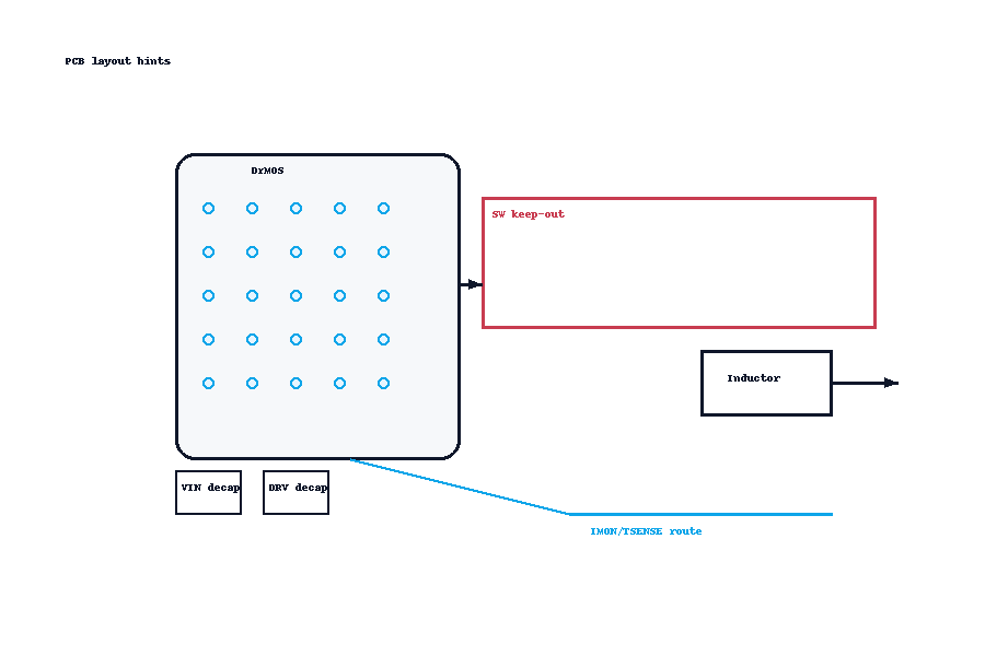
Switching Loop & Decoupling
- SW fencing: Guard the SW polygon with a keep-out; avoid sensitive traces beneath/near the edge.
- Shortest gate/boot loop: Keep BOOT cap and gate-drive return next to the DrMOS pins; minimize loop area.
- Decoupling ring: Place VIN/VDRV (VCC) capacitors tight to pins; short, wide return to exposed pad/PGND.
- Return integrity: Prefer contiguous ground under the power stage; stitch with vias at each cap pad.
Thermal Path & Mechanics
- Via farm: Dense, evenly spaced thermal vias under the exposed pad (tent bottom if needed to prevent solder wicking).
- Copper & stackup: Use thicker copper or parallel planes; spread heat laterally with copper pours tied to pad.
- Inductor placement: Keep the inductor close for a short SW→L run but allow airflow between bodies.
- Airflow alignment: Orient packages and inductors with the primary airflow; avoid shadowing hot spots.
Telemetry: IMON/TSENSE Routing
- Clean corridor: Route IMON/IOUT and TSENSE away from SW; no crossings on adjacent layers without ground shield.
- Kelvin reference: Reference to a quiet ground; add small RC per datasheet near the controller ADC pin.
- Coupling control: Maintain clearance from fast edges (PWM/PG/FAULT); add series resistors if needed.
Do
- Flood copper around pad; stitch to inner planes.
- Keep BOOT/gate returns as short and wide as possible.
- Place VIN/VDRV decoupling on the same side as DrMOS.
- Measure case temp and validate via IR map.
Avoid
- Running signals under the SW edge or in its near field.
- Long, skinny traces for gate, BOOT, or decoupling returns.
- Sparse vias under the exposed pad.
- Routing telemetry parallel to PWM or SW segments.
Want a land-pattern you can reuse for multiple vendors? Get pin-compatible options.
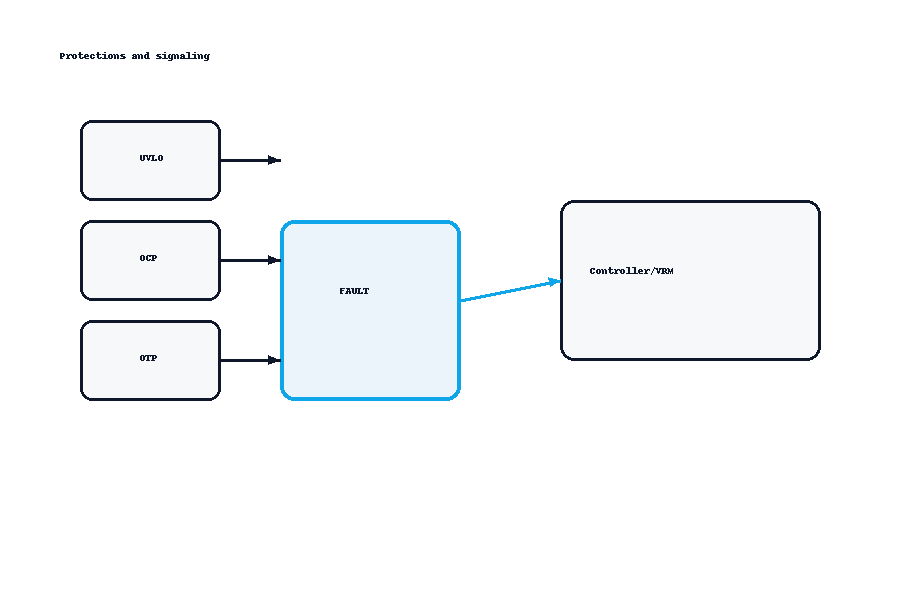
Protections Inside the Package
A modern DrMOS embeds fast protection to contain faults at the package level and communicate status to the controller. Verify trigger paths, thresholds, and how faults clear to avoid nuisance trips or stuck-off rails.
Protection Set & Reset Behavior
- OCP (over-current protection): Cycle-by-cycle limit clamps HS on-time each cycle; latched OCP requires an explicit clear (EN toggle, tri-state PWM, or power cycle). Check trip level and tolerance.
- OTP (over-temperature protection): Trips on internal/packaged sensor; may auto-recover with hysteresis or latch until cleared. Validate at hot soak and airflow corners.
- UVLO (under-voltage lockout): Monitors VDRV/VCC (and sometimes VIN); blocks PWM drive when bias is low to prevent half-drive events. Confirm start/stop thresholds and blanking.
- Shoot-through prevention: Managed dead-time, cross-conduction blanking, and gate interlocks. Verify timing across temperature and process spread.
Minimal Signaling to the Controller
- PG (power-good): Indicates valid operating region; confirm polarity (active-high/low) and driver type (open-drain vs push-pull) and provide the correct pull-up voltage.
- FAULT / ALERT: Aggregates OCP/OTP/UVLO/shoot-through events; define the clear method (PWM tri-state, EN toggle, or power cycle) and debounce/blanking to avoid chatter.
- System aggregation: For board-level fault trees and PMBus reporting, see the PSM/PMBus page.
Protection Verification (Bring-Up)
- Measure OCP trip at cold/room/hot; confirm cycle-by-cycle vs latched behavior.
- Heat to OTP threshold under worst-case airflow; confirm recovery hysteresis or the need for a manual clear.
- Brown-in/brown-out tests for UVLO with logging of PG/FAULT timing.
- Record the clear sequence (PWM tri-state window, EN pulse width, power-cycle hold time).
Need devices with compatible PG/FAULT polarity and thresholds? Get pin-compatible options.
Validation Checklist (Bring-Up & A/B Compare)
Use this checklist to take a DrMOS from first power-on to data-backed sign-off. Cover three operating points, calibrate telemetry, verify timing, and document results for cross-batch and A/B part comparisons.
Power-On Script
- Soft-start: PWM tri-stated at boot; enable phases sequentially; confirm PG default and release timing.
- Three operating points: Light load, nominal load, thermal steady-state (hot). Record Vout regulation and ripple.
- Safety gate: Confirm FAULT clear method (EN toggle / PWM tri-state / power cycle) before stress tests.
Efficiency Grid (Fsw × Iout)
Measure at least a 3×3 matrix for each candidate; keep ambient and airflow constant.
| Fsw \ Iout | Low | Nominal | High |
|---|---|---|---|
| Low Fsw | % | % | % |
| Nominal Fsw | % | % | % |
| High Fsw | % | % | % |
Normalize cabling and shunt losses; log VIN/VOUT, IIN/IOUT, case temp, and airflow in each point.
Waveforms & Timing
- HS/LS gates: Capture rise/fall, dead-time, and shoot-through margin at cold/room/hot.
- SW node: Ringing, dV/dt, diode conduction interval; add snubber/series gate if needed (retest EMI).
- BOOT rail: Verify no droop during transients and at max duty; check UVLO masks during soft-start.
Telemetry & Limits
- IMON calibration: Calibrate offset/slope at three points (≈10%, 50%, 90% Iout); document drift vs temp.
- Limits: Verify OCP type/threshold, OTP trip and hysteresis, and UVLO start/stop; correlate with PG/FAULT timing.
- ADC integrity: Check filter constants and reference routing; ensure no coupling from PWM/SW edges.
Thermal Verification
- Steady-state case temp: Log case and inductor temps at nominal/high load until thermal equilibrium.
- Dual method: IR camera hot-spot map + thermocouple at case; confirm against ΘJA/ΘJC budget.
- Airflow realism: Test intended chassis airflow; note shadowing and fix with spacing/orientation.
Cross-Batch Consistency & A/B Compare
- Test samples from at least two date codes/lots; compare efficiency deltas and timing spread.
- Run the same 3×3 grid for A/B candidate parts; rank by efficiency, peak temp, and fault behavior.
- Store scope shots, CSVs, and thermal images alongside worksheet IDs for traceability.
⬇️ Download: SPS_Bringup_Checklist.pdf
Recommended Test Conditions
- Ambient points: 25 °C and worst-case (e.g., 45–55 °C in chassis).
- Airflow: record LFM or fan RPM/curve; keep constant across A/B runs.
- Instrumentation: 4-wire shunt for IIN/IOUT, calibrated thermocouples, 350 MHz+ scope for SW ringing.
Want us to run the grid and return a ranked shortlist? Submit your BOM (48h).
Real-World Use Cases
-
CPU VR (6–10 phases, 300–600 kHz)
- High thermal density around socket; ensure even airflow.
- Favor low RDS(on) (LS) and solid ΘJC for per-phase current.
- Keep SW loop tight; decoupling on same side as DrMOS.
- Verify dead-time across temp; minimize diode conduction.
- PG/FAULT polarity must match VR enable strategy.
- Run 3×3 efficiency grid; log case temp at steady state.
-
GPU / AI Accelerator (6–12 phases, multi-duct airflow)
- Focus on heat spreading; align packages with airflow channels.
- Prioritize IMON accuracy and drift for telemetry-based limits.
- Balance Qg/Qoss vs EMI; consider snubber if SW ringing rises.
- Distribute inductors to reduce hot-spot shadowing.
- PG aggregation and FAULT clear method defined before stress.
- A/B compare efficiency and max case temp at common airflow.
-
Industrial Servo / Telecom (3–6 phases)
- Expect supply disturbances and wider ambient variation.
- Select wider VIN/VDRV ranges and robust UVLO/OTP.
- Use Kelvin-routed IMON/TSENSE; filter near controller ADC.
- Conservative Fsw for efficiency and EMI margin.
- Thermal vias under exposed pad; thicker copper or inner heat planes.
- Document fault behavior with brown-in/brown-out tests.
FAQs
Concise, engineer-facing answers you can act on. For controller compensation/IMVP policy, see the Multiphase Controller page; for PMBus aggregation, see PSM/PMBus.
DrMOS vs discrete driver + MOSFETs — how do they trade off on efficiency, size, and consistency?
DrMOS minimizes parasitics and loop length in one package, improving efficiency and reducing layout sensitivity. It saves board area and delivers tighter phase-to-phase timing. Discrete stages can be cheaper or handle unusual voltages but demand careful routing, dead-time tuning, and thermal design. Choose DrMOS for fast time-to-first-pass and repeatability at scale.
Why does my DrMOS run hot even when efficiency looks acceptable?
Heat is usually a mix of conduction and switching loss. High Iphase stresses RDS(on); high Fsw raises Qg/Qoss losses and ringing. Inadequate via farms, thin copper, or poor airflow concentrate hotspots. Validate with a 3×3 efficiency grid and dual thermal measurement (IR + thermocouple), then adjust Fsw, pad copper, or part choice.
Should PWM be 3.3 V or 5 V, and how important is tri-state behavior?
Use the controller’s native PWM IO level; confirm DrMOS VIH/VIL and absolute maximum ratings. Mismatched levels may require tolerance checks or level shifting. Tri-state defines safe “both-off” gating for start-up, faults, and phase shedding. Verify the detect threshold, default state, and timeouts so the controller’s policies operate as intended.
How accurate is IMON, and how should I calibrate it across temperature?
IMON accuracy includes scale, offset, and drift. Route with Kelvin reference and filter near the controller ADC. Calibrate at three points—roughly 10%, 50%, and 90% of Iout—while logging temperature. Apply slope/offset corrections in firmware and verify at hot/cold corners. Re-run after layout changes or device substitutions to maintain telemetry fidelity.
What dead-time should I target to avoid shoot-through without hurting efficiency?
Too little dead-time risks cross-conduction; too much pushes current through the body diode, increasing loss and stress. Start with the vendor’s recommended setting, then validate HS/LS gate timing at cold/room/hot. Observe SW diode conduction time and ringing. Fine-tune only if needed; many DrMOS parts handle dead-time internally.
How do UVLO, OCP, and OTP thresholds interact with my controller’s policies?
UVLO prevents half-drive when VDRV/VCC droops; OCP limits current cycle-by-cycle or latches; OTP protects the package with hysteresis or latch. Ensure thresholds and tolerances align with expected inrush, brown-in/out, and thermal conditions. Define clear methods: EN toggle, PWM tri-state, or power cycle to avoid nuisance latched faults.
Can I swap between brands with pin-compatible parts safely?
Yes—if you verify more than the footprint. Match PWM level and polarity, tri-state behavior, IMON/TSENSE scaling, UVLO/OC/OT thresholds, PG/FAULT polarity and driver type, and exposed-pad land pattern. Run an A/B bring-up with the same 3×3 efficiency grid and thermal checks before committing the substitution.
How do I choose Fsw without blowing up losses or magnetics size?
Use a window, not a single point. Higher Fsw improves transient response and reduces inductance, but raises Qg/Qoss loss and EMI. Evaluate at low/nominal/high Fsw with your target inductor, then compare efficiency and case temperature. Keep some margin for aging, airflow variance, and workload burstiness.
What layout practices matter most around the SW node and decoupling?
Fence the SW polygon and avoid routing signals under or near its edge. Keep BOOT and gate returns short and wide. Place VIN/VDRV decoupling on the same side as the DrMOS with tight return to the exposed pad. Stitch ground with vias at each capacitor pad and under the pad.
My PG flickers during brown-out testing. What should I check?
Confirm UVLO thresholds versus your rail droop profile and the PG debounce/blanking time. Check pull-up voltage and whether PG is open-drain or push-pull across phases. Reduce noise on the PWM input and verify controller behavior in tri-state. If needed, add hysteresis or filtering consistent with the datasheet.
How should I filter IMON/TSENSE without corrupting telemetry dynamics?
Place small RC filters near the controller ADC, referenced to quiet ground. Keep cutoff above control-loop bandwidth yet low enough to reject SW-edge coupling. Use Kelvin routing and avoid parallel runs with PWM or SW. Validate with step loads and temperature sweeps to preserve delay and accuracy.
How do I spot counterfeit or refurbished DrMOS devices?
Look for inconsistent top marks, sanding or re-coating, unusual exposed-pad finish, and date-code anomalies. For higher assurance, use X-ray, decap, or AC electrical sampling. Buy from authorized channels and log incoming-inspection photos. Maintain lot traceability and keep A/B thermal/efficiency records to catch outliers early.
Any handling or storage tips to avoid ESD and moisture damage before reflow?
Treat DrMOS as ESD-sensitive: grounded mats, wrist straps, and ESD bags. Follow the MSL rating—store dry, bake if exposure exceeds floor life, and reseal with desiccant. Keep trays flat to protect leads and pad planarity. Record lot and expiration data to correlate reflow outcomes and returns.
Resources & RFQ
Download the worksheet and bring-up checklist, then send us your rail details. We support small batches, rush builds, and cross-brand pin-to-pin substitutions. Optional services include X-ray, decap, and AC electrical sampling.