
Synchronous Buck Controller / Module — Design & Selection Guide
A synchronous buck replaces the rectifier diode with a low-side MOSFET, cutting conduction loss and boosting efficiency—especially for low output voltages and higher currents. This child page focuses on single-phase synchronous bucks; Multiphase VRs, Boost/Buck-Boost, and PMBus/PSM telemetry live on sibling pages.
Introduction & Use Cases
Why synchronous rectification matters—quick math: for 12 V → 1.2 V @ 5 A, duty ≈ 0.1.
With a Schottky diode (Vf ≈ 0.5 V), loss is
P ≈ I * Vf * (1 − D) ≈ 5 * 0.5 * 0.9 ≈ 2.25 W.
Using a low-side MOSFET (Rds_on ≈ 10 mΩ), conduction loss becomes
P ≈ I² * R * (1 − D) ≈ 25 * 0.01 * 0.9 ≈ 0.225 W — about 2 W saved.
MCU/SoC/FPGA cores and I/O; radios and mixed-signal auxiliaries.
PLC/servo controllers, motor boards, sensors, HMIs.
Consider AEC-Q100 parts, cold-crank and EMI constraints.
Choose a synchronous buck when VOUT is low, IOUT is moderate-to-high, and the design is constrained by efficiency, thermal headroom, and EMI predictability.
Need 3 pin-to-pin options or AEC-Q100 replacements? Submit your BOM (48h).
Looking for Boost/Buck-Boost or Multiphase VRs? See Buck-Boost, Boost, Multiphase Controller, or PMBus/PSM.
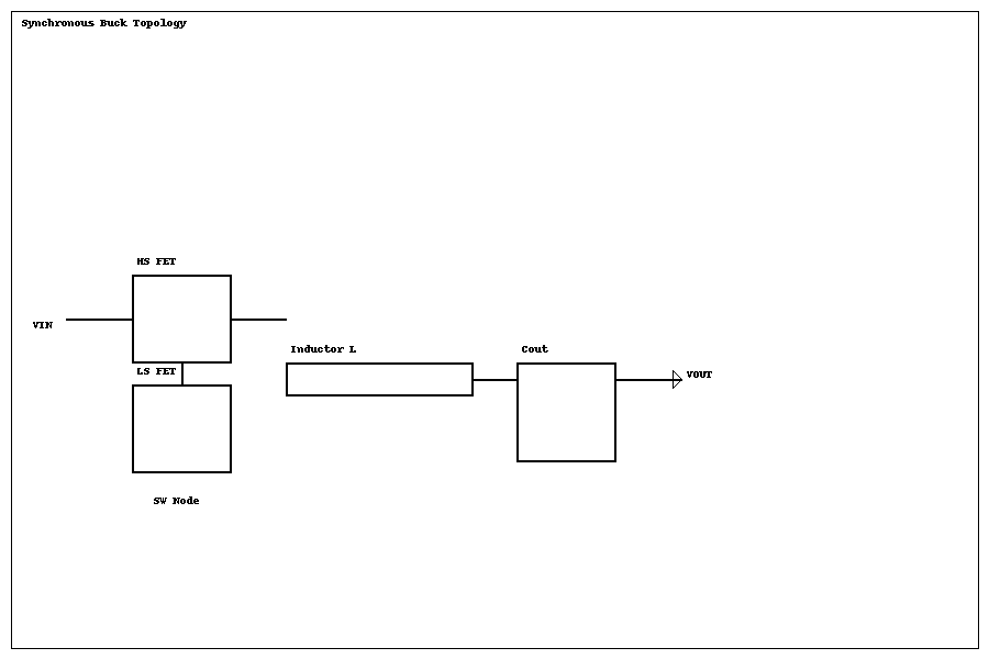
How a Synchronous Buck Works
HS/LS MOSFET roles & the SW node
The high-side MOSFET connects VIN to the inductor; the low-side MOSFET (replacing the diode) provides the return path when HS is off. The SW node swings between VIN and ground as the inductor current remains continuous (CCM) or reaches zero (DCM).
Dead time, body diode, and reverse recovery
Controller dead-time avoids shoot-through. If too long, the LS body diode conducts longer, raising loss and EMI via reverse-recovery charge (Qrr); if too short, overlap current causes heat. Modern controllers use adaptive dead-time to minimize diode conduction without overlap.
CCM vs DCM
In CCM, inductor current never hits zero—ripple is lower and control is simpler, but light-load efficiency suffers. In DCM, current reaches zero—light-load efficiency improves at the expense of ripple and potential acoustic noise. Minimum on-time and valley detection set practical limits for very small duty cycles.
Where efficiency goes
- Conduction loss: I²R in HS/LS FETs, inductor DCR, PCB copper.
- Switching loss: gate charge (Qg), Coss, Qrr events, and driver loss.
- Frequency trade-off: higher FSW shrinks magnetics and improves transient response but raises switching loss and EMI.
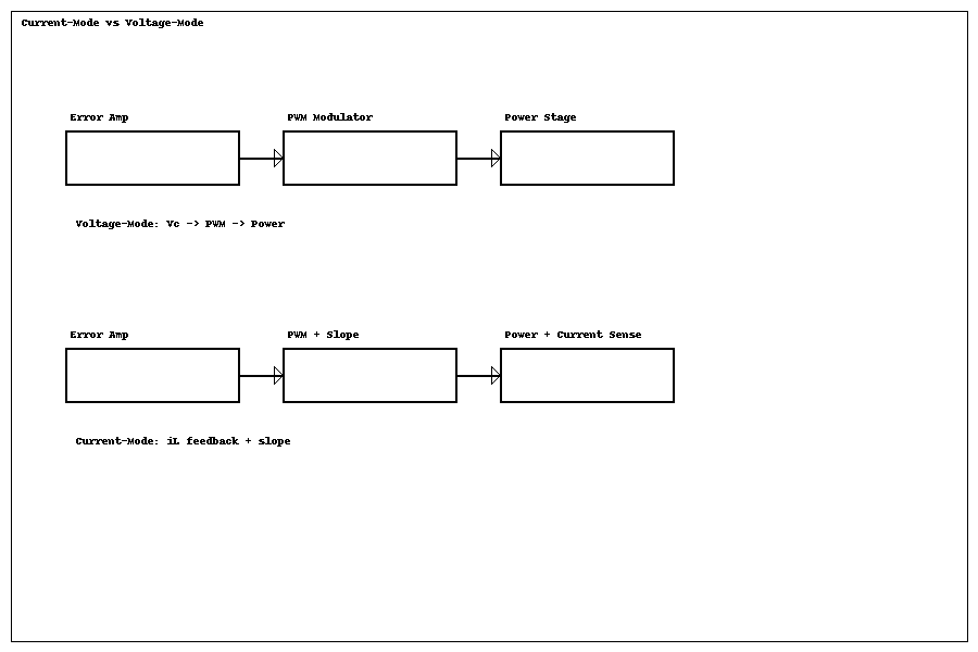
Control Modes & Compensation
Control overview
Voltage-mode offers low noise and predictable duty but can interact with input filters. Peak current-mode embeds a current loop that improves line transient and eases compensation; at duty > 50% you need slope compensation. Valley current-mode / COT can achieve short minimum on-time and fast step response with simple sensing.
Stability targets (pragmatic)
- Crossover frequency
f_c ≈ Fsw / 5 … Fsw / 10 - Phase margin ≥ 50–60°, gain margin ≥ 8–10 dB
- Ceramic outputs (low ESR) often require a Type-III network
Type-II / Type-III placement
LC double pole: ω0 = 1 / √(L·C); ESR zero: ωz,ESR = 1 / (RESR·Cout).
Type-II suits higher ESR or added RC-zero outputs. Type-III places two zeros around the LC double pole, one pole above crossover, and a high-frequency pole for roll-off.
Slope compensation (peak current-mode)
To avoid sub-harmonic oscillation at duty > 0.5, inject a down-slope at the PWM ramp. A practical rule is
m_slope ≥ (m_down − m_up) / 2, or at least half the inductor current down-slope.
Internal vs external compensation
- Internal: faster bring-up and layout simplicity, but limited tuning range across L/C spread.
- External: maximum bandwidth/stability control, ideal for wide VIN/IOUT or tight transient specs.
Feed-forward capacitor (Cff)
Cff in parallel with the upper divider resistor (Vout→FB) improves high-frequency gain and reduces overshoot. Start small (e.g., 10–100 pF) and sweep upward; verify noise coupling and ensure stability at high VIN.

Inductor & Switching Network
Ripple target and initial sizing
Start with ΔIL ≈ 0.2–0.4 · IOUT. For a buck,
D = VOUT / VIN and an initial estimate
L ≈ (VIN − VOUT) · D / (ΔIL · Fsw).
Smaller ΔIL lowers AC loss and ripple but increases inductor size and can limit bandwidth.
Saturation and thermal current
Ensure Isat ≥ IOUT,max + ΔIL/2. Thermal RMS current may limit earlier than Isat;
DCR and winding geometry strongly affect efficiency and temperature rise.
FSW / loss / EMI trade-offs
- Higher Fsw shrinks magnetics and improves transient response.
- But switching loss (Qg, Coss, reverse recovery) and EMI rise; check minimum on-time at high VIN/low VOUT.
- Typical starting points: 400–800 kHz for mid-current rails; verify with your EMI and thermal budgets.
Synchronous vs diode rectification
Synchronous offers much lower conduction loss at low VOUT/high IOUT but requires careful dead-time control; excessive dead-time leads to body-diode conduction and higher Qrr loss. Schottky is simple and robust but loses efficiency quickly at low VOUT—sometimes useful at ultra-light load to suppress audible noise.
MOSFET selection quick notes
Balance Rds_on vs Qg/Coss. Tune gate resistors and driver strength; manage Miller effect, dv/dt, and ringing.
Check package thermal (θJA) in your board stack-up.

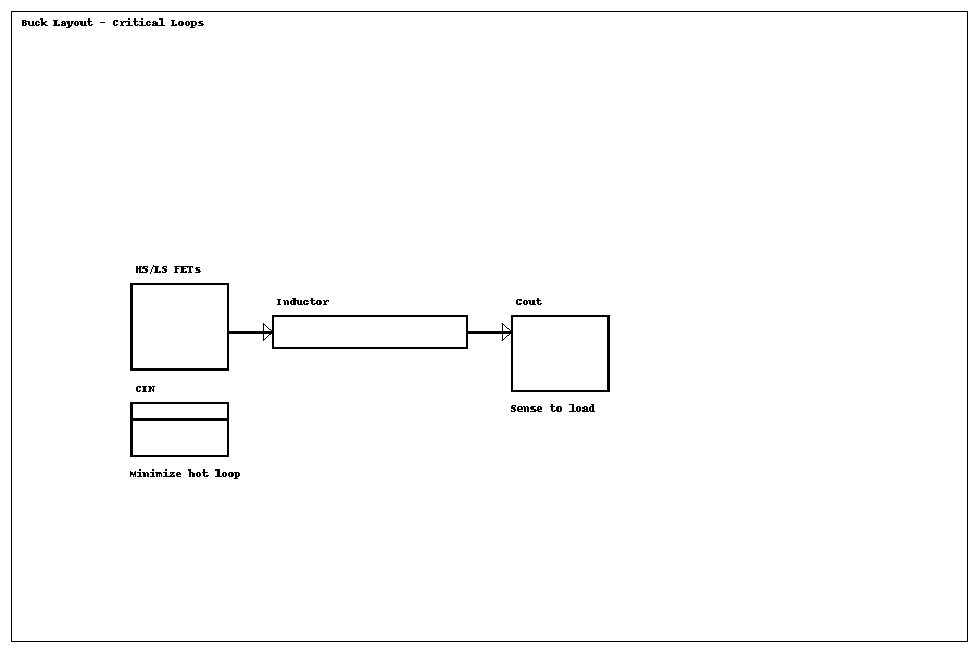
Layout matters next—see the critical switching loop and return paths in Layout & EMI Notes.
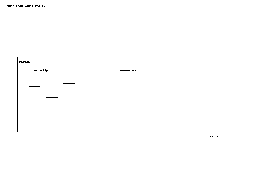
Light-Load Strategy
PFM / skip vs forced-PWM
PFM / skip reduces switching events at light load to cut switching loss—excellent efficiency but higher ripple and potential audible noise. Forced-PWM keeps a fixed switching frequency for low ripple and RF/audio-friendly noise, at the expense of light-load efficiency.
Audible/EMI noise in skip modes
- Mitigations: raise PFM threshold, limit minimum on-time, or enable forced-PWM on sensitive rails.
- Add small post-filtering (RC/LC) or a downstream LDO for audio/RF paths.
- Verify burst frequency minima, ripple (mVpp), and demodulated EMI “birdies”.
Low quiescent current (Iq) & standby
Iq is the regulator’s self-consumption when lightly loaded or idle. µA-class Iq greatly extends battery life in always-on systems. Typical Iq depends on mode and VIN/VOUT conditions—check typical and max ratings.
Mode thresholds & validation
- Set automatic CCM/DCM/skip thresholds after magnetics and
Fsware chosen. - Record wake-up/exit hysteresis, minimum on-time limits, and valley/zero-current detection behavior.
- Confirm no accidental hiccup during normal light load; hiccup is a fault-mode behavior.
Protections & Soft-Start
Over-current protection (OCP)
- Peak OCP: clamps the inductor peak current—fast response, more sensitive to ripple/transients.
- Average/Valley OCP: closer to real thermal load current—robust with large
ΔIL. - Foldback current limit: reduces VOUT under heavy overload/short, minimizing thermal stress.
UVLO / OVP thresholds
- UVLO: defined turn-on/turn-off with hysteresis to prevent chatter during brown-out.
- OVP: protects against feedback faults and load-dump-like events; verify trip/reset points.
- Automotive/industrial: consider cold-crank and load-dump; reverse battery and surge handled by front-end protection.
Over-temperature protection (OTP)
OTP trip/clear points should align with your board’s θJA, copper area, and airflow. Avoid thermal
oscillation by ensuring margin between steady-state temperature and the OTP threshold.
Soft-start & pre-biased startup
- Soft-start ramp controls inrush and overshoot; coordinate with Cff and loop bandwidth to prevent ringing.
- Pre-bias: keep the low-side MOSFET off during ramp if VOUT is already charged; validate power-cycle, brown-out, and hot-reset.
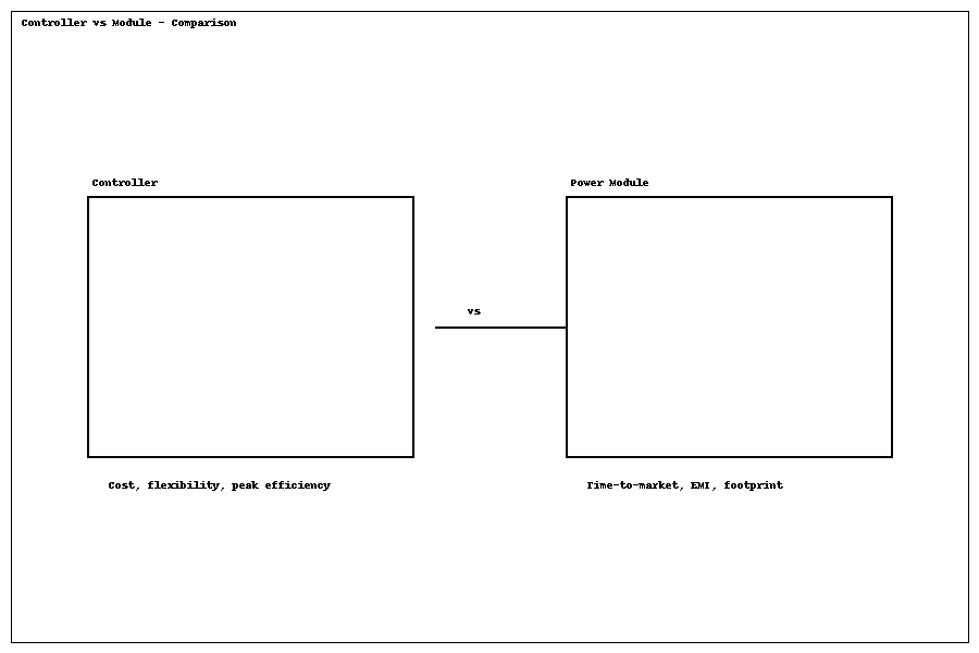
Controller vs Power Module
When to pick a power module (SiP/integrated): you need compressed BOM, predictable EMI/thermal results, compact layout, and faster time-to-market—ideal for small teams or space-constrained boards.
When to pick a controller (PWM + external FET/inductor): you prioritize cost optimization, tunability, and efficiency/thermal limits at extremes (high VIN, high IOUT, very low VOUT). Freedom to choose magnetics and FETs enables the best W/$ at volume.
Comparison matrix
| Dimension | Module (with inductor) | Module (power stage only, no inductor) | Controller (external FET & inductor) |
|---|---|---|---|
| Cost ($/W) | Highest, pay for integration | Medium | Lowest at volume |
| BOM & sourcing | Minimal lines, single vendor | Reduced but still source L/C | Full BOM, multi-vendor |
| Area / height | Small footprint, height depends on inductor | Small footprint, inductor height external | Variable; can be larger but flexible |
| EMI predictability | Best—pre-validated layout/magnetics | Good—hot loop internalized | Depends on your layout & parts |
| Thermal path | Known θJA; easy thermal modeling | Good; external inductor spreads heat | Fully tunable with packages & copper |
| Peak efficiency | Very good within spec window | Good; some FET freedom | Highest with optimized FET/inductor |
| Loop bandwidth / tuning | Limited (often internal comp) | Moderate (some tuning) | Maximum (external comp) |
| Validation effort | Lowest | Low–medium | Highest (but most flexible) |
| Lifecycle / AEC options | Check series longevity | Check stage & passives options | Wide choices incl. AEC-Q100 |
Inductor-included vs power-stage-only
- Inductor-included module: simplest path to success; pay premium and accept limited tunability/height.
- Power stage only (no inductor): hot loop is integrated, but you still choose the inductor/Cout—middle ground for cost/control.
3-step decision
- Time & resources: tight schedule or small team → start with a module.
- EMI/compliance risk: high risk → module; normal → go to step 3.
- Cost/efficiency extreme: extreme VIN/IOUT or cost-sensitive → controller; otherwise prototype both and decide by thermal/EMI.
Design Flow & Quick Worksheet
Six steps from targets to validation
- Inputs/outputs & ripple: define
VIN(min/typ/max),VOUT,IOUT(max), ripple target and transient spec. - Pick Fsw: balance EMI/efficiency/size (often 400–800 kHz to start); mind minimum on-time at high VIN/low VOUT.
- Estimate L / ΔIL: set
ΔIL ≈ 0.2–0.4 · IOUT,D = VOUT/VIN, then
L ≈ (VIN − VOUT) · D / (ΔIL · Fsw)as an initial value. - Power stage & drive: trade
Rds_onvsQg/Coss; size gate resistors/driver; check thermal path andθJA. - Compensation draft: target
f_c ≈ Fsw/5…Fsw/10, phase margin ≥ 50–60°; with ceramic output caps prefer Type-III; add modest Cff if needed. - Test & calibrate: load/line steps, pre-biased start, short-circuit/hiccup, thermal sweep/derating, EMI and acoustic noise.
Brand & Part Examples
Below are series-level examples for single-phase synchronous buck controllers, integrated regulators (with FETs), and power modules. We can provide 3 pin-to-pin alternatives within 48h—submit your BOM at the bottom.
| Brand | Controller Families | Integrated Buck Families (with FETs) | Power Module / SiP Families |
|---|---|---|---|
| TI | TPS40xxx, LM51xx | TPS62xxx, TPS56xx | TPSM82xx, TPSM53xx |
| ST | L67xx, L59xx | L698x, L798x | STPMIC / selected µSiP series |
| NXP | PF / PF8xxx (PMIC buck control), VR55xx (auto PMIC) | PF50xx / PF81xx PMIC buck rails | Module availability varies by platform |
| Renesas | ISL81xx, RAA48xxxx | ISL85xx, RAA21xxxx | ISL82xxM, RAA22xxM |
| onsemi | NCP15xx / NCP81xx (incl. NCV variants) | NCP31xxx / NCV series | NCPM series (per VIN/IOUT) |
| Microchip | MIC21xx, MIC28xxx | MIC23xxx, MCP1650x, PMIC buck rails | MIC2830x, MIC43xx |
| Melexis | Focused on sensors/actuators; dedicated synchronous buck families are limited—ask us for cross-brand replacements. | ||
* Series names are illustrative and commonly encountered. For lifecycle (NRND/EOL) and pin-compatibility, use the RFQ form. See also: Controller vs Power Module.
Submit your BOM (48h)Layout & EMI Notes
Core principles
- Minimize the hot loop: keep VIN → HS FET → SW → CIN extremely tight; place input MLCCs next to the power stage.
- Return path: provide a low-impedance path for high di/dt currents; single-point tie AGND to PGND.
- Split grounds: route FB/COMP/RT on clean AGND, then join to PGND at the IC’s recommended star point.
- Sensing: take FB from load or Cout pads; keep it away from the SW copper; use differential routing if available.
- Hot vs cold nets & shielding: keep SW copper contained; fence with ground pour/vias where needed.
Placement priorities
- Input MLCCs (CIN) hugging VIN/GND pins and HS/LS devices.
- Inductor close to the power stage for a short SW→L→Cout path.
- Output capacitors placed to tightly close the loop.
- COMP/FB RC near the IC and far from SW.
Vias, copper & coatings
- Use multiple stitching vias for grounds and high current paths; expose thermal pads with copper pours.
- Avoid unnecessary splits near SW; prevent slot antennas.
- Ensure solder mask coverage on high dv/dt regions; keep BOOT/gate traces short and direct.
EMI & damping
- Add RC snubbers to tame SW ringing if needed; verify their thermal impact.
- Check input π-filter interaction with control loop—avoid creating an under-damped peak.
- Reserve pads for A/B tests (snubbers, gate resistors, small RC across inductor).
θJA.
FAQs
Current-mode vs voltage-mode — which should I choose?
Why is Type-III compensation common with ceramic outputs?
How much slope compensation do I need in peak current-mode?
Should I add a feed-forward capacitor (Cff)?
How do I select ΔIL and the inductor value?
D = VOUT/VIN and estimate L ≈ (VIN − VOUT)·D/(ΔIL·Fsw), then refine for thermal and transient goals. Smaller ΔIL reduces ripple but enlarges L; larger ΔIL improves bandwidth yet raises EMI. See Inductor & Switching.
Which limits first — inductor Isat or thermal Irms?
Isat ≥ IOUT,max + ΔIL/2, but also model DCR and core loss at your Fsw and ripple. Validate with temperature rise on your board, not only datasheet curves. More guidance in Inductor & Switching.
PFM/skip produces audible noise — how to mitigate?
What does “low Iq” mean, and how do I verify standby?
Peak vs average/valley OCP — when, and why foldback?
Soft-start and pre-biased startup — what should I check?
Module or controller — how do I decide quickly?
What crossover frequency and margins should I target?
fc ≈ Fsw/5 … Fsw/10 with phase margin ≥ 50–60° and gain margin ≥ 8–10 dB. Ceramic outputs often benefit from Type-III networks. Verify across VIN/IOUT and temperature. More in Control & Compensation.
How does Fsw affect efficiency and EMI?
How do I minimize the hot loop and manage return paths?
Resources & RFQ
Downloads
We return 3 pin-to-pin alternatives within 48 hours, including lifecycle notes.
Submit Your BOM & Contact
Prototype with a module, or cost-down with a controller—your call. We’ll suggest both paths.